Seven-segment readout displays high, low, open, and pulse.
By R.M. STITT

--------------
PARTS LIST:
C1,C3-25-NF, 6-volt tantalum electrolytic capacitor
C2-220-pF ceramic disc capacitor
D1 thru D4-Signal diode (IN914 or similar)
D1S1--Common cathode seven-segment LED display (Opcoa SLA-7 or similar)
IC1-Retriggerable monostable multivibrator (74122)
IC2-Hex inverter (7405)
IC3-Quad two-input NAND gate (7400)
Q1,Q3--Npn silicon switching transistor (2N3904 or similar)
Q2--Pnp silicon switching transistor (2N3906 or similar)
The following are 1/4-watt, 5% tolerance resistors
R1, R2-47,000 ohms
R3, R4, R5, R14, R 15-10,000 ohms
R6-22,000 ohms
R7 thru R13-180 ohms
Misc.--Printed circuit board; 7 1/4" x 1" inner diameter CPVC plastic tubing; s/s' or 1/2" diameter hardwood dowel stock (see text); one red- and one black-booted alligator clips; 72" length of No. 18 test lead cable; 6d finishing nail; solder; etc.
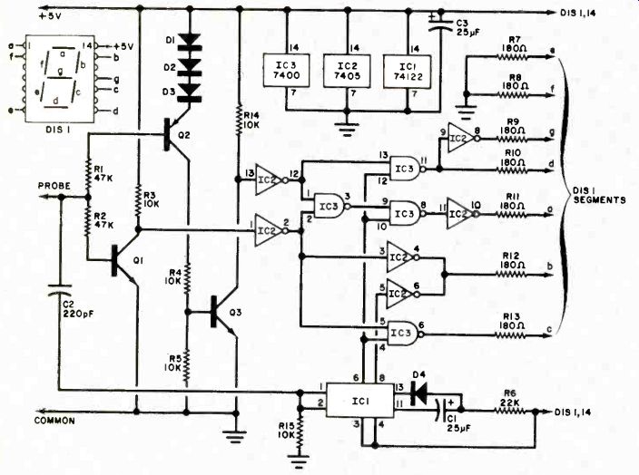
Fig. 1. Schematic diagram of the logic probe. Transistors Q1 and Q2 are
in comparator circuits which set the logic levels. IC2 and IC3 decode the signal.
THE LOGIC probe is almost a necessity in checking digital circuits. Usually the probe detects and discriminates between high-level, low-level, and pulse conditions at various points in a digital circuit. The results are then displayed on miniature lamps or discrete light-emitting diodes.
If you want a more advanced logic probe, try the one described here. It does what the conventional probe does, but has the additional capability of being able to sense an open circuit or an out-of-tolerance high or low logic level. And the indicator is a single seven-segment LED display.
The four possible test conditions are shown as actual letters on the seven-segment display.
The letters are: H (high logic level), L (low logic level), o (open), and P (pulse). This type of display makes testing faster and improves accuracy in reading the results.
How It Works. Shown in Fig. 1 is the logic probe's schematic diagram.
Transistor Q1 functions as a voltage comparator and buffer with a threshold of approximately 0.6 volt.
Transistor Q2 and diodes D1, D2, and D3 function as a voltage comparator and buffer with an approximate 2.4-volt threshold. These thresholds are slightly wider apart than is standard for TTL devices, thus providing a safety margin.
Resistors R4 and R5 and transistor Q3 shift the level of Q2 to make it TTL compatible. The outputs of the two comparator circuits are further buffered and conditioned by IC2, the high (H) and low (L) outputs of which are decoded by the remaining circuitry.
Assuming that the point under test is either at a constant high or a constant low, the end result will be an H or an L displayed on D1S1.
In the event of any pulse activity at the point under test, one-shot multivibrator /C1 will trigger and generate a P (for pulse) on D1S1. If a single pulse occurs at the test point, IC1 will still cause a P to be displayed, but only for about 0.5 second. (The probe is capable of "capturing" pulses as short as 10 ns in duration.) Any time the probe tip is not touching a point in the test circuit or is touching a point that is electrically isolated from the circuit, D1S1 will display an 0. Furthermore, any logic level that is within the range set by the comparators will also result in an o being displayed.
In operation, H indicates a high TTL state (greater than 2.5 volts); L indicates a low TTL state (less than 0.6 volt); o indicates an open circuit or an out-of-tolerance TTL state (high impedance or less than 2.5 volts but greater than 0.6 volt); and P indicates a pulse train or single pulse.
Construction. When assembling the probe, parts layout and lead dress are not particularly critical. The test prod lead should be kept as short and direct as possible through the junction of R1 and R2.
To keep the electronic assembly as compact as possible, a printed circuit board is a must for component mounting . The etching and drilling and component placement guides are shown in Fig. 2. Since you will be making your own double-sided board and will not be able to plate through the holes, it is important to solder connections on both sides of the board. Consequently, you must install the components in a set sequence. Install and solder into place R7, R9, R13, and R15 before you install R8, R10, R11, and R12. Likewise, install C2 before C1.
All remaining components can be installed in whatever sequence you desire. (Note: The component placement guide shown in Fig. 2 is the view from the top, or component, side of the board. The items to be installed first are indicated in phantom in Fig. 2.) After wiring the circuit board, solder a 1" (25 mm) length of insulated wire to the pad under DIS1 nearest the end of the board. The free end of this wire goes to the probe's test tip. Prepare the ends of two 36" (about 1-m) lengths of test-lead cable, and solder one end to the +5-volt and ground pads on the board.
Now, cut a 3/4" long by 5/32" deep (19 X 3.8-mm) window 1/2" (13 mm) from one end of the tube. Use CPVC tubing; it has thinner walls to provide a slenderer assembly than is possible with ordinary PVC tubing. CPVC tubing is available from most hardware and building supply stores.
You can fabricate the end caps for the tube to the dimensions given in Fig. 3 by turning on a lathe or whittling with a knife 5/8" (16-mm) diameter hardwood dowel stock. If you don't have access to a wood-turning lathe or don't relish whittling, you can fashion blunt end caps from 1/2" hardwood dowel stock and use small screws to hold them in place. In either case, drill a 1/4" (6.5-mm) diameter hole through the rear end cap and a hole just large enough to require force fitting a 6d finishing nail into it through the front end cap.
Pass the power leads for the probe through the hole in the rear end cap.
Connect and solder a red-booted alligator clip to the +5-volt and a black-booted alligator clip to the ground cables.
Test the probe by connecting its power cables to the +5-volt and common buses of a known good circuit and touching the probe lead to the +5-volt bus, common bus, and a point in the circuit where there are pulses.
When the power leads are initially hooked up, the display should indicate 0. Touching the probe lead to the +5-volt and common buses should cause an H and an L to be displayed, respectively. With the probe lead touching a point in the circuit where pulse activity is taking place, the display should indicate a P. The circuit board is deliberately wider than the inside diameter of the plastic tube. To get the board into the tube, you will have to deform the latter.
To do this, place the tube between two blocks of wood in a vise and very carefully close the vise just enough to permit the board to slip into place. Before Spening the vise, make certain that the display is centered in the window of the tube.
File or grind the point of the finishing nail to a sharp tip, contouring it like a standard test-probe point. Drive the nail into the front end of the cap, leaving about 1/4 of the nail head free.
Locate the free end of the probe tip wire coming from the circuit board.
Strip away about 3/8 of insulation from the wire, wrap the exposed wire around the nail head, and drive the nail home in the end cap. Push both end caps into the tube (and secure them with small screws if necessary), and the probe is ready to use.
Fig. 1
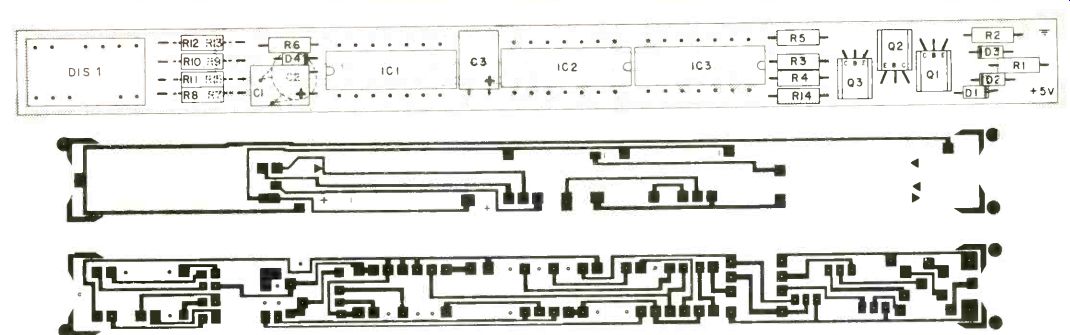
Fig. 2. Etching and drilling guides and component layout .for pc board are
above.
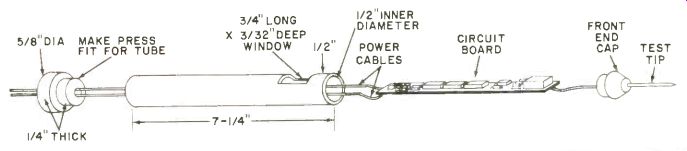
Fig. 3. Diagram shows how to assemble the probe. Be sure display shows in
the window.
Also see:
Talk Over A Sunbeam With A "Photophone"
Link | --Automatic Diode Checker
Measure RPM of Rotating Elements with the IC Photo Tachometer