Transistor Characteristics Which Can Be Tested
Characteristics of transistors which can be measured include DC beta, AC beta, shorts, leakage, opens, bandwidth, linearity, polarity (PNP or NPN), internal capacitance, noise level, and maximum permissible operating currents and voltages. Only a few of these characteristics can be tested in an electronic service shop, because of practical limits of test equipment and technicians' time.
Several simple methods of testing some characteristics of transistors were given in Section 8.
Testing of shorts, leakage and opens is understood best by thinking of the transistor as three inter connected diodes, as shown in Fig. 2. Forward and reverse resistance of the three junctions can be measured with an ohmmeter by testing one junction, then reversing the polarity of the leads and measuring again. This method demands some experience in interpretation, and, unfortunately, when applied to non defective silicon types, infinite resistance is indicated by most of these tests. However, some opens, shorts and most leakage can be detected using this method.
Each diode junction of a transistor also can be dynamically tested for its ability to rectify, by use of the circuit shown in Fig. 3. The ideal waveform for a good junction is a right angle. A short produces a vertical line, and an open produces a horizontal line. These tests can be made on in-circuit transistors; however, the accuracy will depend upon the circuit characteristics. Also, collector-emitter tests are not as definite as we might desire, and leak age indications are not very sensitive.
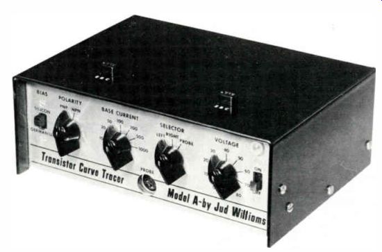
Fig. 1 Jud Williams Model
A transistor curve tracer, one of at least three commercially produced curve tracers now available. Unit shown here simultaneously applies one step of a staircase waveform of current to the base of a transistor and a parabolic voltage to its collector. Emitter-collector current (voltage dropped across emitter resistor) is used to drive the vertical deflection of a scope and the collector voltage provides horizontal deflection. The resultant waveform is a "family of curves" which reveals the degree of control the base exercises over emitter-collector current, levels of leakage between junctions and AC gain, or beta (ratio of base and collector currents). Two three-prong sockets on top of unit are for out-of-circuit testing of transistors. Three-prong probe which is plugged into PROBE socket on front panel of unit is used for in-circuit testing. Connections to scope are located at rear of unit.
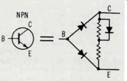
Fig. 2 Equivalent circuit of an NPN transistor shows three interconnected
diodes which represent the relation ships of the three elements of a transistor-emitter,
base and collector. Resistance testing of these "equivalent diodes" reveals
positive information about the diode action of the junctions (front-to-back
ratios) and the junction to-junction leakages (reduced resistance). The equivalent
circuit of a PNP transistor is the same as that shown here, except the polarity
of the diodes is reversed.
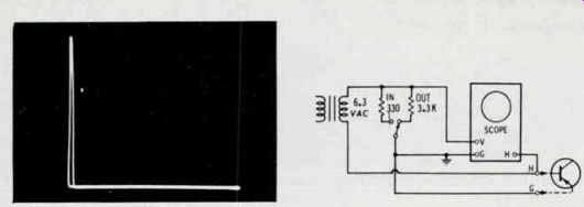
Fig. 3 Schematic of a simple method which permits testing of the diode junctions
in a transistor using a scope as the readout. A right angle is the ideal waveform
for base-emitter and base-collector junctions.
Fig. 4 The ability of the base to control the resistance of the collector-emitter
circuit can be tested by this simple test unit, which is connected to an ohm
meter.
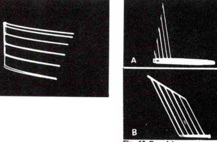
Fig. 5 DC beta is the ratio of static base current to static collector current.
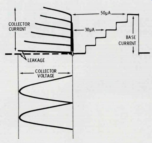
Fig. 6 A typical family of transistor curves showing the relationship between
the DC "staircase" base current and the DC parabolic collector voltage.
The collector voltage varies from zero volts to maximum and back to zero again
during the duration of each step of the staircase. Collector-emitter leakage
can be read by the tilt of the zero base current curve compared to the true
zero line on the scope graticule.
Turn-on and turn-off tests in which the collector-emitter junction is measured with an ohmmeter are true measures of transistor actions.
Of course, no accurate calibration is possible. The basic circuit for such tests is shown in Fig. 4.
DC beta testers accurately measure the DC, or static, gain of a transistor by adjusting the base current to achieve a known collector current; the base current then is measured on a meter whose scale is calibrated in DC beta. The smaller the base current required, the higher the beta. A simplified schematic of this method is shown in Fig. 5. In actual commercial instruments, only one meter is used, with switching for the various shunts. Other switch functions are used for polarity reversal, leakage, calibration, etc. Also, provision usually is made for the beta tests to be made at various amounts of collector current.
This is desirable because transistors provide different betas at different collector currents. For example, one transistor measured a beta of 180 at 1 milliamp and a beta of 240 at 10 milliamps. Many commercial transistor testers have provision for measuring beta in-circuit. I will not comment on this be cause to date I have not had an occasion to perform these tests.
Testing Transistors With Curve Tracer And Scope
Dynamic transistor curve tracers are beginning to be heralded as the best solution to some of the short comings of the preceding tests. Follow with us as we thoroughly check out the performance of the Jud Williams Transistor Curve Tracer, Model A (photo in Fig. 1). The curve tracer applies a "stair case" waveform of base current to the base of the transistor, and during each step of the staircase a DC voltage that varies from zero to maximum and back to zero again is applied to the collector of the transistor. Collector current vertically deflects the scope beam, and collector voltage provides horizontal deflection.
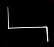
Fig. 7 Curve produced on a solid-state scope as a result of protective zener
action in the horizontal sweep circuit of the scope. Many scopes will overload
when the COLLECTOR VOLTAGE control is set to produce higher voltages.
False curves are the result. See the text for ways of eliminating such horizontal sweep overload.
Fig. 6 shows the relationships between the waveforms applied to the transistor and the resultant "family of curves" produced by a normal transistor. The family of curves shows collector voltage and current at zero base current and at five steps of increasing base current.
Tilt of the "zero base current" curve (the longest one) is an indication of collector-to-emitter current not controlled by the base. This un controlled current is a direct indication of collector-to-emitter leakage.
How To Connect The Scope And Obtain A Curve
Three wires extend from the rear of the curve tracer cabinet. The black lead connects to the ground post of the scope, the white lead to the horizontal input terminal or binding post, and the red lead to the vertical input. Usually, it is more convenient to use the regular scope probe. If the probe has direct and low-capacitance functions, use the direct position, to avoid unnecessary mathematics when measuring transistor beta.
Rotate the horizontal selector knob on the scope panel to the position marked "EXT", "H INPUT" or "HORIZONTAL INPUT". With both the curve tracer and scope turned on and the VOLTAGE control of the tracer turned up partially, a horizontal line should be seen on the screen of the scope. The horizontal width of this line should vary when both the VOLTAGE control on the tracer and the horizontal gain control on the scope are adjusted.
Scope intensity, focus and centering should be adjusted normally.
No locking adjustments are necessary, because the scope receives both horizontal and vertical deflection voltages from the curve tracer.
Preset the BASE CURRENT switch to 10-ua, the SELECTOR switch to LEFT position and the VOLTAGE control to about 20 volts. Plug into the left socket on top of the tracer a small three-lead transistor which is known to be good. Be certain the leads are inserted in the correct socket holes.
---------------
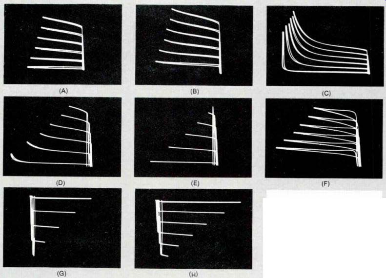
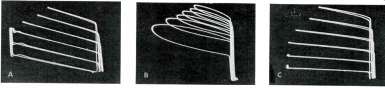
Fig. 8 Normal variations in curves of non-defective transistors.
(A) Family of curves for a 2N411 PNP germanium transistor. BASE CURRENT control set for 10 ILA per step of the staircase, and VOLTAGE control set at 20 volts PP. (B) Curves produced by same transistor, but with BIAS switch erroneously set for silicon instead of germanium. (C) Curves produced by same transistor, but with VOLTAGE control set at 70. Avalanche leakage occurs at about 50 volts. (D) Curves produced by same transistor, but with BASE CURRENT control set at 50 /IA, VOLTAGE set at 30, and scope vertical gain reduced. (E) Curves produced by same transistor and conditions as in (D), but, because COLLECTOR VOLTAGE is set at only 20, only 5 curves are produced on scope. (F) Curves of an old type 2N301A PNP germanium power transistor. Notice how leakage tilts the "zero base current" curve. Also note the loops in each curve, which indicate poor frequency response and internal heating. (G) Family of curves of a small NPN silicon transistor with BASE control set at 10 uA and COLLECTOR set at 15 volts. This transistor produces about 50 percent more gain than the one in (A). (H) Curves produced by same silicon transistor, but with VOLTAGE control increased to 25, to produce all 6 curves.
------------------------
Between two and six curves, de pending on the transistor, should appear on the scope. Wrong setting of the POLARITY switch will cause an "L" or "J" waveform or a vertical line. Select the position of the POLARITY switch which produces a normal curve; the polarity of the transistor then can be read directly from the position of the switch.
Adjust the vertical and horizontal gain controls and the centering controls for a waveform of sufficient size to be seen easily. Fewer changes in centering will be produced by adjustment of the various controls if the scope vertical circuit is set for the AC function.
Overload of the horizontal deflection circuit in the scope is relatively common when the voltage control is positioned to high settings. Fig. 7 shows the bent ends of the waveform produced by over load in one brand of solid-state scope (caused by zener protection of the FET used as horizontal amplifier). To test your scope for this possibility: 1) Operate the tracer and scope as usual, except do not plug in a transistor; 2) Progressively increase the setting of the VOLTAGE control on the tracer while reducing the scope width with the horizontal gain control; 3) A vertical corner or a brighter area at either end of the horizontal line indicates scope overload. Such overload can not be considered a transistor or scope defect, because more input is applied to the horizontal amplifier of the scope than is necessary for full horizontal deflection.
Elimination of scope overload is very simple. The manual for the Jud Williams curve tracer says to insert a 1 meg-ohm (or higher, if needed) resistor between the white wire from the tracer and the horizontal input of the scope. If you are plagued by pickup of a powerful local broadcast station which rides on top of the waveform, as we are in our locality, a 5-to-1 or 10-to-1 fixed voltage divider might minimize the interference. Values of 470K/47K-ohm perform well with the solid-state scope.
Normal Variations Of The Curves
Gain, leakage, avalanche voltages, linearity and many other characteristics of transistors vary widely. Consequently, many variations in the waveshape of curves obtained from individual transistors of the same nomenclature and brand can be expected, in addition to the larger variations obtained from transistors of different types and/or brands.
However, the mere production of a family of curves, regardless of minute variations and/or abnormalities, in most instances can be considered absolute proof that the base of the transistor is controlling the collector current and, consequently, the transistor probably is functioning relatively normally. In other words, presence or absence of the family of curves is, for all practical considerations, a valid "go/no-go" indication.
Many of the normal out-of-circuit curves are shown in Fig. 8. Notice carefully the settings of the curve tracer controls, which are listed for your guidance.
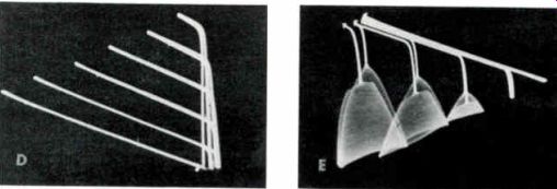
Open Circuits and Leakages
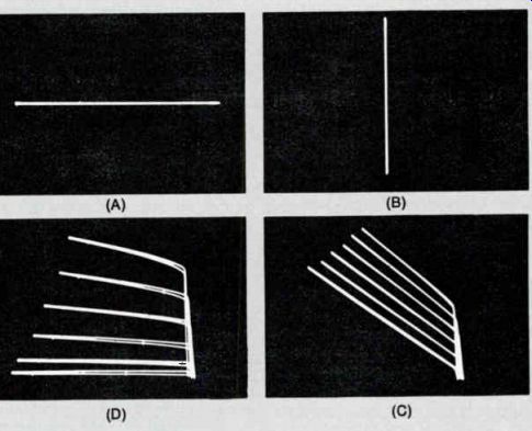
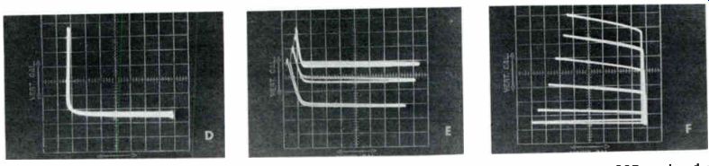
An open in any element, a base emitter short, or no transistor plugged into the curve tracer will produce a straight horizontal line on the scope, as shown in Fig. 9. A vertical line is caused by a collector emitter or a base-collector short.
Leakage tilts the horizontal lines of the curves. Fig. 9 shows the curves produced by transistors with various values of leakage.
Mistakes Cause Wrong Curves
Improper curves can be caused by mistakes in plugging in or connecting the transistors or improper adjustment of the curve tracer controls. Some of the resultant snares possible are shown in Fig. 10.
------- Fig. 9 Curves produced by defective transistors.
(A) A single horizontal line is caused by a base-emitter short or an open element.
(B) A single vertical line is caused by a base-collector or collector-emitter short (C) Curves of a 2N408 PNP germanium transistor with a 1.8K-ohm short between collector and emitter, or a 180K-ohm short between base and collector. Notice the tilt of all the curves. (D) Non-linearity near the "zero base current" curve of a 2N408 caused by a base-emitter short of 10K ohms.
-----------
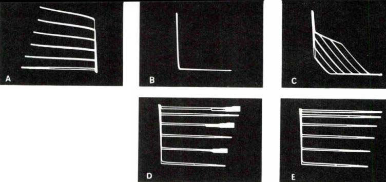
Fig. 10 Abnormal curves caused by improper connections and/or adjustments.
(A) At first analysis, this is a normal-appearing curve; however, the collector
and emitter of the transistor where interchanged. A large base current of 100-uA
was required to produce the curve, indicating very low transistor gain. (B)
Some variation of a right angle is obtained when the POLARITY switch is reversed.
(C) A right angle and false curves caused by operation of a NPN silicon power
transistor with the polarity switch set for PNP and the base current increased
to 500 A. (D) The same NPN silicon power transistor operated correctly with
BASE CURRENT of 10-uA, but with the SILICON BIAS control turned to one end,
causing a "gremlin" on alternate lines. This is a factory adjustment
which can be touched up, if needed. Slight adjustment of the bias control eliminated
the spurious response. (E) Curves produced by same transistor reveals non-linearity,
also caused by a wrong setting of the SILICON BIAS control.
--------
Comparison of Tests Of Defective Transistors
For comparison, I tested several defective transistors with 1) the curve tracer, 2) with a good commercial beta tester and 3) by use of the standard series of ohmmeter tests. The results then were compared for accuracy and speed. The findings are included in the following paragraphs.
Fig. 11 shows the curve tracer waveform and the results of the other two methods. The beta tester disclosed that the DC beta was slightly low, but the transistor was otherwise okay. Analysis of the ohmmeter readings indicated collector-to-emitter leakage, while the curve tracer revealed low gain and poor linearity. All three methods indicated that the transistor was not completely normal, but the results from the curve tracer were obtained quicker and were more absolute.
The curves in Fig. 12 indicate high transistor beta, or gain; however, the slope of the "zero collector voltage" side of the curves was excessive. Base-emitter forward resistance measured normal (110 ohms) on an ohmmeter, but the base-collector forward resistance was 1.2K ohms, nearly ten times the normal value. The beta tester indicated that the beta was 170 at 1 milliampere, and that the leakage was normal. Both the ohmmeter and the curve tracer revealed a defect in the transistor, but the curve tracer revealed it quicker.
It's possible to try too hard to obtain a curve; in such cases the result usually is a false curve, as shown in Fig. 13. Ohmmeter measurements indicated that the transistor had an open emitter. The beta tester indicated "no collector current." The two curves produced by the curve tracer are false ones obtained by increasing the setting of the COLLECTOR VOLTAGE control which, in turn, increased the height of the waveforms.
----------------- Fig. 11 These curves are nearly normal for a NPN
silicon type except for some non-linearity, but low gain was indicated when
the base current had to be increased to 20 1,A to obtain a wave form of the
usual height. Beta measured 42 at 10 milliamperes, with no noticeable leakage.
The collector-emitter forward reading was 20K ohms and the reversed reading
only 24K ohms.
Fig. 13 Two false curves produced by an NPN transistor with an open emit ter. Base-collector was 80 ohms; base emitter indicated infinity on ohmmeter tests. (A) Tested as an NPN, with base current of 100 , E A. (B) Tested as a PNP, with the base current at 500 1,A.
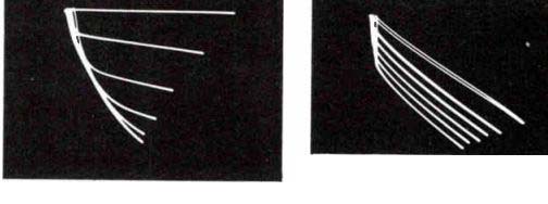
Fig. 12 Excessive slope of the left side of the curve. Beta was 170, with
normal leakage. The forward resistance of base-emitter junction was a normal
110 ohms, but the base-collector measured 1.2K ohms. Fig. 14 Curve here shows
low gain (base 20 u-A) and severe leakage. Beta was 67 with collector-emitter
leakage.
Ohmmeter tests indicated collector emitter forward resistance of 1300 ohms; the reverse resistance was 3000 ohms. All three test methods produced accurate indications in this case.
------------
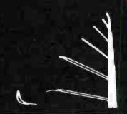
Fig. 15 Except for the peculiar leakage pattern on the "zero base current" curve,
these curves indicate a normal PNP germanium transistor. Ohmmeter tests were
good, and beta measured a high 300.
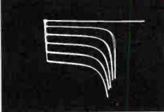
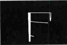
Fig. 16 Three different kinds or degrees
of avalanche leakage. (A) Base current of 50 u-A was necessary to produce
this normal-size waveform, indicating low gain in this NPN silicon transistor.
Ohmmeter tests were normal, except for excessive base-collector leakage. Beta
was 37, with normal leakage indicated. (B) Curves of this NPN silicon transistor
indicate very high gain (base current 10-uA) and a sharp avalanche at 10 volts.
Ohmmeter readings were normal. Beta was a very high 400 at 10 milliamperes. Only
the curve tracer showed any sign of a defect in this instance. (C) A NPN silicon
transistor with an indicated beta of 140 and normal leakages and ohmmeter readings.
The transistor had so much avalanche the corner of the curve moved down and touched the bottom curve when the collector voltage was increased to 20 volts.
---------
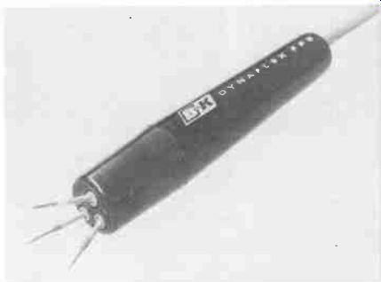
Fig. 17 Probe (for testing transistors on circuit boards) supplied with the
Jud Williams Curve Tracer.
--------------
All three test methods correctly indicated high leakage in another transistor, whose family of curves is shown in Fig. 14. However, tests with the curve tracer required less time.
A "zero base current" curve of a 2N1303 germanium transistor is shown in Fig. 15. This curve indicates leakage with a few volts of collector voltage, no leakage with a relatively higher level of collector voltage, followed by normal avalanche leakage. (Another transistor of the identical type did not produce the unexpected dip in the base line.) The beta reading was a high 300, and leakage was normal. Ohmmeter readings seemed normal. Only the curve tracer found this defect.
Two extreme avalanche conditions are shown in Fig. 16. The curve at (A) shows low-gain avalanche leakage on all of the curves except the "zero base current" curve, which usually is the first to bend when the COLLECTOR VOLTAGE control is advanced. A beta of only 37 and normal leak ages were indicated by the beta-type tester, while an ohmmeter test indicated excessive collector-base leak age.
The family of curves shown in Fig. 16B reveals a sharp avalanche leakage at only 10 volts PP. Many circuits use more DC voltage than this, and under such conditions the transistor would act as if it had a collector-emitter short. Normal ohmmeter readings and a very high beta reading of 400 at 10 milliamperes with normal leakage would seem to indicate that the transistor was entirely normal. Only the curve tracer revealed the true defect, a voltage limitation.
Another transistor with lower gain exhibited similar avalanche symptoms. Fig. 16C shows how the avalanche corner extended down to meet the "maximum base current" curve when the collector voltage was increased to 20 volts.
Because many transistors are soldered to the circuit board, in circuit testing can save valuable time ordinarily spent unsoldering and removing the transistor. Also, the possibility of damaging the transistor is reduced.
The Jud Williams Transistor Curve Tracer Model A is reported to have the capability of finding defective transistors in most circuits.
One plug and cable supplied with the tracer has three small clips on the end for connection to out-of circuit transistors or diodes which do not fit the sockets on top of the tracer, or for in-circuit connection to any transistor where space permits. A three-tip B&K probe (see Fig. 17), with cable and connector, also is supplied. Each of the three sharp tips is free to swivel in a circle, and each is spring loaded to retract partially into the probe when under pressure so that solid electrical contact can be maintained against any copper foil circuit board.
Each tip has a color band, to identify the base, emitter and collector connections.
The family of curves produced by in-circuit tests are radically different than those produced with the transistor out of circuit. Mr. Williams advocates that these displays be called "signature patterns", and suggests that they be included by the manufacturers in their service data, or added by technicians to their PHOTOFACT schematics after the pattern for each normal in-circuit transistor has been deter mined.
Capacitances and inductances in the circuit often make loops out of the curves, while resistances cause the curves to tilt as though the transistor were leaky. For example, a 0.25-mfd capacitor (without any transistor) connected between the base and collector clips of the tracer probe produces an approximately ...
-------------
Fig. 18 A near-ellipse is produced by connection of a .25-mfd capacitor between
the base and collector clips of the probe R MAN 10M UP,SIEP Transistor Curve
Tracer
Model A-by Jud Williams
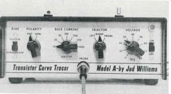
Fig. 19 Front panel controls of the Williams curve tracer.
(A) Curves of a
2N408 PNP transistor in a resistance coupled audio amplifier. Base-emitter
conduction in the following transistor amplifier stage causes what appears
to be an avalanche condition at the end of the zero base current line.
(B) Signature pattern curves of a 2N408 PNP transistor in an output circuit
which includes a transformer in the collector circuit, but with the speaker
disconnected. BASE CURRENT set for 10 A. (C) A PNP audio output transistor
with a transformer and speaker connected to the collector circuit produced
curves resembling out-of-circuit ones.
BASE CURRENT switch set for 20 u-A. (D) Signature pattern curves of a mixer-oscillator PNP transistor in a portable radio resemble those of a leaky out-of-circuit transistor. However, a BASE CURRENT setting of 1000 1 ,,A was necessary because of loading by the circuit. (E) The same transistor and circuit as in (D) gave this set of false curves which include pulses of RF oscillation when the POLARITY switch was changed to the incorrect NPN.
Fig. 20 Examples of in-circuit transistor curves.
---------------------
... oval shape, as shown in Fig. 18 Higher setting of the BASE CURRENT switch (often to the full 1000 u-A position) and the VOLTAGE control are required to over come the loading of some circuits.
By comparison, most transistors can be tested out of circuit with only 10 µA of base current. Locations of these controls on the panel of the curve tracer are shown in Fig. 19.
Distortion of the signature pat terns often can be reduced by connecting together the positive and negative voltage supply terminals of the circuit under test (no power is applied to the circuit during in circuit tests with the tracer). Several typical signature patterns of good in-circuit transistors and one interesting pattern resulting from the use of wrong polarity are shown in Fig. 20. It is clear that effective in-circuit testing of transistors can be done with this curve tracer, especially if comparisons with known good transistors are used to aid interpretation of borderline cases.
Testing Other Solid-State Components
Go/no-go tests of solid-state components. such as diodes, zener diodes, SCR's and FET's, also can be made with the Williams curve tracer, although the instrument was primarily designed for transistor testing. Typical waveforms obtained when these other solid-state devices were tested out-of-circuit are shown in Fig 21.
The base-emitter junction of soli con transistors exhibit zener action when tested as a diode. This is a positive way of identifying silicon alloy type transistors, since germanium types do not exhibit zener action.
Inside the Jud Williams Transistor Curve Tracer
A simplified schematic of the Williams curve tracer is shown in Fig.'"). A pulsating DC staircase waveform is applied to the base of the transistor under test, through fixed resistors selected by the BASE CURRENT switch. During the time each step of the staircase is present at the base, a pulsating DC voltage of parabolic waveshape is applied to the collector. This voltage starts at zero, increases to the maximum determined by the setting of the VOLTAGE control, then decreases
------------------
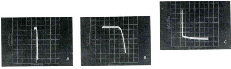
Fig. 21 Out-of-circuit tests of diodes, FET's and SCR's. (A) Curve of a power
supply diode connected between the emitter and collector clips of the external
probe. POLARITY switch is set for NPN. Reverse the polarity and a horizontal
line should be obtained, indicating an open circuit. (B) The right angle
curve of (A) widened by increasing the horizontal gain of the scope. A good
diode should have this horizontal part of the angle, while a shorted diode
will produce only a vertical line. (C) Curve produced by a zener diode connected
with its cathode to the emitter clip and its anode to the collector clip.
The POLARITY switch should be set for PNP. The base emitter junction of a
silicon transistor shows the same zener curve. Incorrect setting of the POLARITY
switch produces the normal diode curve shown in (A).
(D) Leakage and avalanche voltage are best shown with the base disconnected, but emitter and collector connected normally. This 2N410 transistor was not leaky, but showed avalanche at about 28 volts.
(E) A FET of unknown characteristics produced this unusual waveform. It seems advisable to test a known-good FET as a standard before testing a suspected one.
(F) Surprisingly, one SCR produced a set of curves very similar to those of a power transistor.
---------------------
… to zero. Because there is one parabola for each step of the 6 step staircase, and the parabola frequency is 120 Hz, the repetition frequency of the staircase pattern is 20 Hz and some visual flicker is noticed on the pattern.
A dynamic visual display of the emitter current at zero and five increasing base current steps is created on the screen of any scope by: 1) applying the voltage developed across the emitter resistor to the vertical amplifier and 2) by applying the collector voltage to the horizontal sweep amplifier.
Although it is seldom necessary in practical servicing to measure accurately the DC beta (the height of the curves tell the approximate gain), such a reading is possible.
Calibrate the gain of the vertical amplifier of the scope so that each vertical division of the graticule is 0.1 volt. Then with the BASE CURRENT switch set for 10 WA, each division represents a beta of 100, when the space between the two desired curves is measured. Fig.23 shows transistor curves for a beta of 40. Each division represents a beta of 50 when the base current is 20 WA, etc.
Several minor trade-offs in the curve tracer design prevent the curves displayed from being true base current-vs-collector current graphs, such as those found in transistor manuals. Collector-emitter current is measured by the voltage drop across an emitter resistor, and the voltage there (see Fig.24) is degeneration, which subtracts from the base signal and makes the display slightly more linear. This was done so you can use your normal service scope and avoid the expense of obtaining a special scope with an ungrounded vertical amplifier.
Inversion of the vertical waveform (negative voltages go up, positive go down) is the result of this small compromise.
Horizontal sweep for the scope is taken from the parabolic voltage at the collector of the transistor under test. Therefore, changing the setting of the VOLTAGE control also changes the width of the wave shape on the scope; width can be restored by use of the horizontal gain control. This apparently was done so that a shorted transistor will cause a vertical line, and so a right angle will result from diode and zener diode tests.
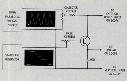
Fig. 22 Simplified schematic of the Williams curve tracer showing the polarity
of waveforms required to test a PNP transistor.
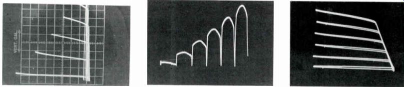
Fig. 23 Curves of a transistor measuring a beta of 40. Calibrate the scope
for .1 volt per vertical division on the graticule, then with the BASE CURRENT
switch set for 10 u-A, each division between the curves represents a beta
of 100; at 20 u-A each division represents a beta of 50. In this example, the
BASE CURRENT switch was set for 50 u-A, therefore each division represents
a beta of 20.
Fig. 24 Waveform across the emitter resistor when the sawtooth horizontal sweep in the scope is used instead of the parabolic horizontal sweep supplied by the curve tracer.
Fig. 25 A sloping zero-collector-voltage side of the curves is the result of experimentally taking the horizontal deflection voltage for the scope from the parabolic supply before the VOLTAGE control.
------------------
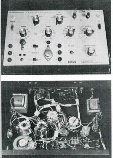
Fig. 26 Front panel layout and the internal wiring of the Eico 443 Semi conductor
Curve Tracer.
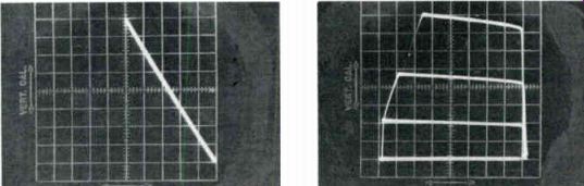
Fig. 27 Calibrate the scope for transistor beta tests with the Eico 443 by
adjusting the horizontal gain, vertical gain and the centering controls on
the scope for a 5-by-8 division diagonal line.
Fig. 28 Typical of curves obtained using the Eico 443 are these curves of a non defective PNP transistor which measures a beta of 60. Adjust the beta knob until the total height of the waveform is 8 divisions, then read the beta from the dial calibration.
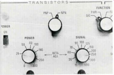
Fig. 29 Power and signal beta calibrations on the transistor-testing side
of the curve tracer.
------------------
The effect on the family of curves when the horizontal sweep for the scope is taken from the parabolic supply before the VOLTAGE control is shown in Fig. 25. The reason for the slanted zero-collector voltage side is that before collector current can flow, the collector voltage must exceed the base voltage (both voltages relative to the emitter). As the base voltage is increased at each step of the staircase, more collector voltage must be applied before current can flow. This actually produces a more accurate set of curves.
These explanations of the minor trade-offs are not intended as criticism, but are given for anyone who really wants to understand completely the electronic principles involved in this curve tracer.
Using The Eico 443 Transistor-Diode Curve Tracer
Another solid-state curve tracer suitable for use in electronic servicing shops is the Eico 443; both the front panel and the internal wiring are shown in Fig. 26 . The design of this tracer seems to be somewhat different than that of the Jud Williams tracer previously de scribed, and, consequently, so is the resultant pattern.
One strong feature of the Eico 443 is the accurate series of tests for diodes, including reverse leak age, maximum PIV and voltage drop in the forward direction.
Four combination binding post/ banana plug jacks are provided on the rear of the cabinet, for connection to a scope. It appears, from the function and spacing of the posts, that the tracer can be plugged directly into the binding posts of the Eico 465 DC scope by the use of four male-to-male banana plug adapters. A 10-by-10 division graticule for use on any scope is included.
The Eico 443 is available in either kit or wired form. We built our sample from the kit and en countered no problem; the tracer worked on the first try.
Testing Transistors With The Eico 443 A zero base current line and three steps of base current are supplied by the Eico unit; thus, four curves are displayed. All small, or "signal", transistors are tested with 10 volts applied to their collectors and a maximum current of 12 milliamps.
Power transistors are tested separately, using another beta-calibrated scale at 10 volts of collector voltage and a maximum of 1 ampere.
Pre-setting of the vertical and horizontal gain controls of the scope by means of standard voltages from the curve tracer is necessary if calibrated readings are to be obtained.
Use these steps for maximum accuracy of readings:
• Connect leads (not supplied with the unit) from the binding posts on the tracer to the matching vertical and horizontal inputs on the scope.
• Slide the POWER switch to OFF and plug in the power cable of the tracer.
• Slide the diode TEST-CAL switch to TEST and the transistor TEST CAL switch to CAL; then turn the FUNCTION switch to SIG for small transistors or PWR for power transistors.
• Slide the POWER switch to ON.
• Select the DC function of the scope, if the scope is thus equipped.
Calibrate the scope by using the vertical and horizontal gain controls and the centering controls to produce a diagonal line 5 divisions wide and 8 divisions high, as shown in Fig. 27.
• Change the transistor TEST-CAL switch to TEST, and the polarity switch to either PNP or NPN, ac cording to the type of transistor you wish to test. If the transistor polarity is not known, try both positions after a transistor is connected; use the one that produces a family of curves.
• Connect the transistor to be tested either by using test leads (not supplied with the unit) or by plugging it into one of the two different sockets. Position the A-B transistor selector switch correctly.
• Measure the DC beta by turning either the POWER or SIGNAL beta knob (according to which type was selected by the FUNCTION switch) until the total height of the pattern (meaning all curves) is 8 divisions, as shown in Fig. 28. Use centering controls as needed. Read the beta from the dial calibration, as shown in Fig. 29.
Several typical curves of abnormal transistors are shown in Fig. 30. Leakage, if any, is shown by the tilt of the zero base current line.
--------------
(A) A NPN silicon transistor with excessive leakage that causes the curves to be tilted.
(B) These curves of a NPN small-signal transistor show excessive leakage, and a beta below 15 (because the curves cannot be adjusted to 8 divisions high). (C) Another NPN small-signal transistor with a beta measuring over 500, but with avalanche at a low collector voltage and excessive leakage.
(D) The forward resistance of the base-emitter junction measured on an ohmmeter a normal 110 ohms, but the base-collector resistance was an abnormal 1.2K ohms. Notice the sloping zero-collector-voltage side of the curves. Beta measured less than 15 on the Eico curve tracer. This is the same transistor tested in the February '71 issue of ELECTRONIC SERVICING in Fig. 12 on page 43. A meter-type tester gave a beta reading of 170 for this defective transistor.
(E) Excessive leakage is indicated in these tilted curves of a PNP power transistor, and the beta tested only 25.
(F) A high beta of over 500 was measured on this NPN silicon small-signal transistor. However, the avalanche at only 10 volts would prevent satisfactory operation in many circuits.
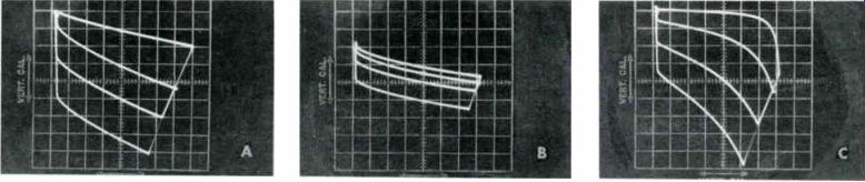
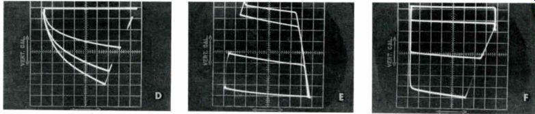
Fig. 30 Typical curves obtained from defective transistors.
----------------------
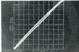
Fig. 31 Scope calibration for diode measurements requires the vertical gain,
horizontal gain and the centering controls on the scope to be adjusted for
a 10-by-10 division diagonal line.
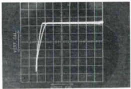
Fig. 32 The diode true PIV rating shown here is 700 volts, because the horizontal
line is 7 divisions wide before avalanche occurs and the VOLTS-DIV PIV switch
was set to 100.
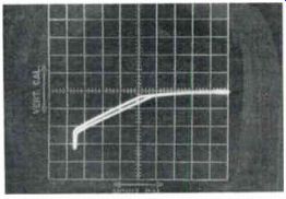
Fig. 33 This zener diode should be rated at 8.5 volts, because
the VOLTS DIV PIV switch was set to 1.
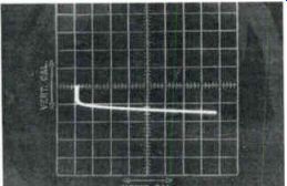
Fig. 34 A forward voltage drop of .75 volt at 800 milliamps is measured by
this diode curve.
Testing Diodes With The Eico 443
A different scope calibration is needed for diode tests:
• Slide the diode TEST-CAL switch to CAL position.
• Rotate the VOLTAGE ADJUST control to minimum (CCW).
• Turn the FUNCTION switch to REV position.
• Adjust the vertical and horizontal gain controls of the scope for a diagonal line across 10 divisions, as shown in Fig. 31.
• Slide the diode TEST-CAL switch to TEST. The HV neon bulb above the switch should flash on and off.
• Turn the CURRENT switch to 10-ua, and the VOLTS/DIV PIV switch to an appropriate scale, such as 10 for a detector diode or 100 for a power supply rectifier.
• Connect the diode to be tested. (Observe polarity markings.)
• Press the PIV TEST button and advance the VOLTAGE ADJUST control. The horizontal line should move to the left until, at a definite voltage reading, a vertical line is formed on the left terminus of the horizontal line; the height of the vertical line will increase with CW movement of the VOLTAGE AD JUST control, as shown in Fig. 32.
Use the centering control of the scope to position the extreme right end of the horizontal line on the right border line of the graticule.
• Read the maximum PIV by the number of divisions from the right end of the trace to the vertical angle line. Multiply the number of divisions by the setting of the VOLTS/DIV PIV switch. Don't be surprised if the PIV of many diodes measures better than the manufacturers' ratings.
A horizontal line indicates an open diode, and a vertical line a shorted one. A horizontal line also can indicate that the VOLT/DIV PIV switch is set too low.
Zener diodes are measured the same way, except the VOLTS/DIV PIV switch is set to a lower scale in anticipation of what the zener voltage should be. See Fig. 33 for the curve produced by one zener diode.
Forward tests of diodes use the same scope calibration as for PIV tests. Use this procedure:
• Turn the VOLTAGE ADJUST control completely down (CCW).
• Change FUNCTION switch to Fig. 35 Base-to-emitter voltage (without a transistor) in the Eico 443 curve tracer shows zero and three steps of base voltage.
FWD position.
• Set the CURRENT switch for 10 or 100 mA/DIV, according to the expected rating of the diode.
• Slide the diode TEST-CAL switch to TEST position.
• Connect, or insert into the test clips, the diode to be tested.
• Increase the VOLTAGE AD JUST control (do NOT press the PIV test button) to produce a horizontal waveform similar to that in Fig. 34.
Position the vertical portion of the trace on the left borderline of the scope graticule, with the trace initially starting on the zero voltage (horizontal) line. The vertical divisions are 0.5 volts each (many silicon rectifiers will measure about .7 or .8, as shown). A vertical line indicates no current (an open diode). How The Eico 443 Works The voltage applied between base and emitter during beta tests is shown in Fig. 35. There are zero and three different steps of voltage, but they are not in sequence. This accounts for the faint lines across the ends of the curves.
Conclusion
A 2N410 PNP transistor was measured for beta by both curve tracers and a good commercial meter-type beta tester. The meter measured a beta of 42 at 10 milliamps and 38 at 1 milliamp. The Eico 443 indicated a beta of 60, and the Jud Williams tracer showed a beta reading of 40. Since all three instruments applied different voltages to the transistor under test conditions, we believe the degree of difference is satisfactory. After all, the DC beta of a transistor varies according to the conditions under which the transistor is operated, and an exact beta is not essential in service work.
------------------------