A whole group of special circuits has been developed for dealing with binary mathematics. Mathematical operations include addition, subtraction, multiplication, division, raising to a power, etc. Many of these operations can be performed with relative simple adder circuits. Other operations require more complex programs.
Even when operations are fairly simple, much effort has been made to develop special circuits and methods to reduce the time needed to complete an operation or to minimize the amount of electronics required. These circuits are beyond the scope of this guide, but a few of the basic circuits will be discussed. These include adders, comparators, and a true/complement generator.
ADDERS
Binary addition follows the same rules as decade addition, except that things happen a lot quicker. In decade systems, each element or decade of a number represents any one of ten different levels or quantities (that is, 0, 1, 2, 3, 4, 5, 6, 7, 8, or 9) ; whereas in binary systems, each element represents only two levels ( 0 or 1). Thus, in Fig. 7-1A, the four-decade decimal number can have any value from 0000 through 9999, while the four-bit binary number shown in Fig. 7-1B, can have any value from 0000 through 1111. The 4-bit binary number can represent 16 levels ( 0 through 15), while the 4-decade number can count up to 9999 (including 0), which identifies 10,000 levels.
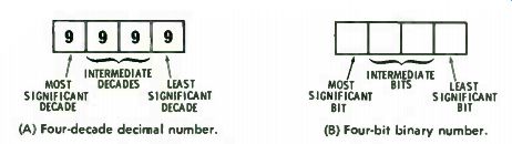
(A) Four-decade decimal number. (B) Four-bit binary number.
Fig. 7-1. Representation of numerical displays.
The decade number system is far more efficient in terms of information content; the binary number system is more suited to electronic systems. Circuits can easily distinguish between two levels of signal but are subject to greater and greater error if they are asked to distinguish between 3 levels, 4 levels, etc.
Two binary numbers can be added as indicated in Fig. 7-2.
Number A, consisting of 4 bits, is to be added to number B, also 4 bits long. When number A = 0000 and number B = 0000, the sum ( E) is also 0000, as shown in Fig. 7-2B. The sum of 0000 and 0001 is shown to be 0001. Then, when adding binary number 0001 to binary number 0001, we find that the space for the Least Significant Bit can no longer show the result by itself.
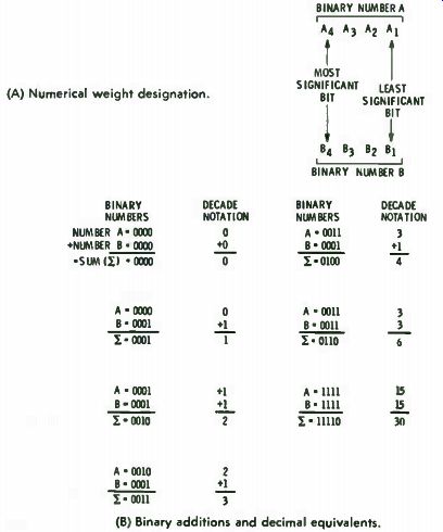
(A) Numerical weight designation. (B) Binary additions and decimal equivalents.
Fig. 7-2. Addition of binary numbers.
Another space or the next most significant bit must be called into use. In other words, the slot or bin for the Least Significant Bit has filled up and overflowed into the next most important bin. ( The same sort of overflow occurs in decade systems when 1 is added to 9, 2 to 8, etc.; the bin overflows and you generate a carry into the next bin.) Similar but more extended carries occur when you add larger numbers, as in Fig. 7-2B. Note that the addition of binary number 1111 and binary number 1111 (both 4-bit numbers) creates a 5-bit number, which means that this operation could not be performed correctly in a system using only 4-bit numbers.
Consider just the Least Significant Bit, numbers A1 and B1 in Fig. 7-2A. Note that this bin can, by itself, correctly represent the sum of 0 + 0 and 1 + 0; it cannot, by itself, represent the sum of 1 + 1, which requires two bits to give a binary 10.
Therefore, any circuit that is required to add two one-bit numbers must be capable of generating a 2-bit output. The Least Significant Bit in such an output is called the sum, and the Most Significant Bit is called the carry.
When adding the least significant bits of two numbers, we only have to deal with two bits, since the carry will by definition always be 0. Such circuits are called half-adders. Circuits that deal with bits having more weight than the least significant bits must handle the carry from the previous stage. These circuits are called full-adders. The operation of addition will be clarified by considering some specific circuits.
Two- Bit Full Adder The 2-bit full adder type 5482/7482 circuit shown in Fig. 7-3A will add two 2-bit numbers and generate the proper carry.
The numbers to be added are inputs A2, A1 and inputs B2, B1.
The output ( Fig. 7-3B) is the sum of the two numbers plus a carry bit to show whether the second bin has overflowed or not.
Line 1 of the truth table ( Fig. 7-4) indicates the addition of 00 to 00. Consider first the case where A1 and B1 are the least significant bits of a number. For this condition, we do not have a carry bit from a lower-level addition, and input CTN is always zero.
With A1 = B1 = Cu.; = 0, Gates 1, 2, 3, and 4 are all closed.
The output of Gate 5 is a 1 and the output of Gate 6 (I I) is 0.
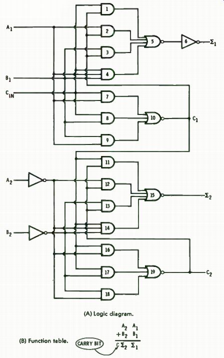
(A) Logic diagram. (B) Function table.
Fig. 7-3. Two-bit full adder.
Also, Gates 7, 8, and 9 are closed so the output of Gate 10 = 1.
With A2 = B2 = 0, we note that Gate 14 has all 1’s as inputs and is therefore open; thus, NOR Gate 15 is satisfied and its output (12) is 0. We note also that Gates 16, 17, and 18 are all open and thus output Co = 0.
The circuit, therefore, has generated the correct output for the specified input.
Line 2 of the truth table indicates the addition of 01 and 00. With Gates 7, 8, and 9 still closed as in the previous addition, the output of Gate 10 is a 1; therefore, Gate 2 has all is as in puts, Gate 5 is 0, and Gate 6 is 1. The rest of the gates have the same status as in the previous addition.
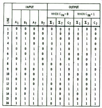
Fig. 7-4. Truth table for Fig. 7-3.
A line-by-line analysis of the circuit can be carried out to verify the truth table for all input states of Ao, A1 and Bo, B1 . When the two bits to be added are not the least and next least significant, the carry bit from a lower-level addition must be handled. When the carry bit from a lower level is 0, the circuit will operate as described above. When the carry bit is 1, then the circuit must operate as indicated for the second set of outputs in the truth table-that is, when CON = 1. Considering line 1 in the truth table, with Co N = 1, we see that Gates 7, 8, and 9 are closed, Gate 10 is a 1, Gate 1 = 1, Gate 5 = 0, and II = 1.
Again, the circuit can be analyzed line by line to verify the truth table.
Note the use of inverters to turns Os into is ( and vice versa)
to make the truth table come out right. This type circuit design is perfectly all right as long as the circuit works correctly for all conditions, and as long as the propagation delays introduced
by such extra stages do not interfere with the timing requirements of the system.
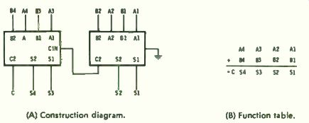
(A) Construction diagram. (B) Function table.
Fig. 7-5. Four-bit addition using two 2-bit adders.
Four- Bit Adder
Two 2-bit adders can easily be combined to form a 4-bit adder as shown in Fig. 7-5. However, the circuit for a 4-bit binary full adder is also available in a single device as shown in Fig. 7-6 ( a type 5483/7483 circuit). The circuit is the same as in Fig. 7-5, except that the carry bit from bin 2 to bin 3 is made internally and not brought outside the package. Also, carry C4 represents the carry across four bits. Four-bit adders can be combined to make 8-bit adders, 16-bit adders, etc.
Gated Adders
The two adders so far discussed add two numbers as soon as the information is received. A gated, 1-bit, full adder (type 5480/7480), is shown in Fig. 7-7.
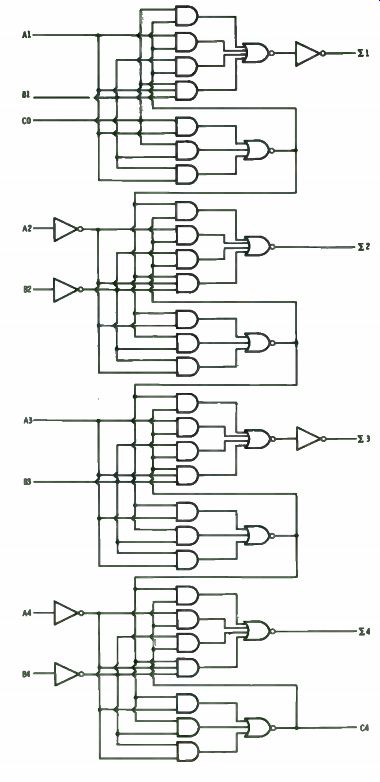
Fig. 7- 6. Four- bit adder logic diagram.
First, ignore Gates 11, 12, 13, 14, 15, and 16. Compare the remaining portion of the circuit with the A1 B1 CI S portion of Fig. 7-3A. The circuits are identical, except that the inverted carry and the inverted sum outputs are brought outside. The inverted carry is labeled C - , 1 7 but is the same as C1 of Fig. 7-3A. Thus, the truth table for Fig. 7-3 applies to the adding circuit of Fig. 7-7 ( except that inputs A2 and B2 and outputs 12 and C2 do not apply, and an output for C1 must be added). The gating portion of Fig. 7-7A consists of diode-transistor logic ( DTL), which is fully compatible with TTL logic. DTL allows use of the wired- os connection, which is forbidden in TTL except for special circuits. In any case, Gates 12 and 15 actually use a permanently-wired connection, although they perform the OR-logic function as indicated in Fig. 7-7B. As a consequence of this arrangement, when input A* is used, inputs
A1 and A2 must be connected to ground. Thus, Gate 11 will be high but will follow input A*, staying high if A* is high. Conversely, when A1 and A2 are used as inputs, input A* must be left open. The same rules apply to inputs B1 , B2, and B*. The gated adder can be used to perform subtraction as well as addition.
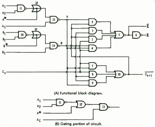
(A) Functional block diagram.
(B) Gating portion of circuit.
Fig. 7-7. Gated full adder.
Fig. 7- 6. Four- bit adder logic diagram.
TRUE/COMPLEMENT CIRCUIT
In binary mathematics, subtraction is usually performed by taking the complement of the number to be subtracted and adding it to the other number. An end-around carry or other mathematical process is then applied so that whatever sub traction algorithm is being used is satisfied, and the answer comes out right.
What is the complement of a number? In decimal notation, a 1-digit number can have any value from 0 through 9. When the number slot is empty, the number contained in the slot is 0, and the number of units that can be added to the slot with out it overflowing is 9. When the slot contains 5 units, the number of units that be added without overflowing is 4. The number of units that can be added to the slot without causing over flow is the complement of the number already in the slot. Thus, 9 is the complement of 0, 4 is the complement of 5; 5 is the complement of 4; etc. The key number in the above system is 9, and the complements are called the nine's complements.
In binary mathematics, a slot can hold only a 0 unit or a 1 unit. Thus, the complement of 0 is 1 and the complement of 1 is 0. The complement is obtained by changing the 0 to 1 and the 1 to 0. As the number of bits is increased to 2 and more (that is, A2 A1 Ao), the same rule holds for a straight binary sequence where binary 000 means no units and 111 means all slots ( of a 3-bit number) are full. For special binary codes, such as excess-3 and excess-2, the complement of a number is not necessarily obtained by changing all is to 0s and all 0s to is. In these cases, more complicated definitions of complement are required.
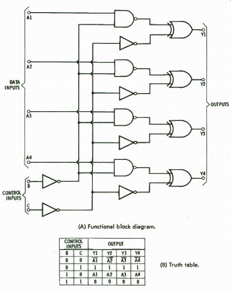
(A) Functional block diagram. (B) Truth table.
Fig. 7-8. Four-bit, true/complement, zero/one element circuit.
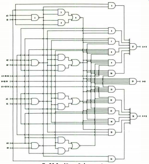
Fig. 7-9. Four-bit magnitude comparator.
In any case, the need arises to generate the complement of binary words and numbers. Fig. 7-8 shows a 4-bit true/complement, zero/one element circuit (monolithic circuit types 54H87, 74H87) that will generate the complement of a number or will pass the number through unchanged. Further, the circuit will also generate all is or all Os. The circuit can be used to load registers in addition and subtraction schemes, or preload counters, etc., in other applications.
Circuit operation is straightforward and is summarized in the truth table in Fig. 7-8B. With B = C = 0, the outputs give the inversions ( the complements) of the input bits. With B = 0 and C = 1, the outputs are all 1; with B = 1 and C = 0, the outputs are the same as the inputs; with B = C = 1, the outputs are all 0.
COMPARATOR
The need often arises to compare one digital number with another. Is number A larger than B, equal to it, or smaller? If B is smaller than A, for example, a digital control system might be required to keep adding pills to a bottle. If A equals B, the system might be told to stop. If B should exceed A, an alarm might sound. Many mathematical equations can be solved in a similar manner.
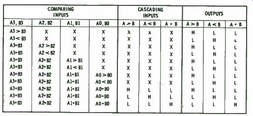
Fig. 7-10. Truth table for Fig. 7-9.
A 4-bit magnitude comparator ( type 5485/7485) is shown in Fig. 7-9. Two 4-bit words, A0 A1 A2 A3 and B0 B1 B2 B3 are applied. Consider bits A3 and B3. Since these are the most significant bits, Word A will be greater than Word B if A3 is greater than B3; that is, if A3 = 1 and B3 = 0. Similarly, Word A will be less than Word B if A3 = 0 and B3 = 1. If A3 = B3, the decision as to whether Word A is greater or less than Word B depends on bits A2 and B2. The same considerations apply to the next two levels of bits. For the two words to be equal, the bits must match on every level.
In normal operation, the inputs marked A < B, A =- B, and A > B are held high. With A3 = 1 and B3 = 0, Gate 1 goes to a 1 driving Gate 3 to a 1, which drives Gate 4 to 0. Gate 4, in turn, drives Gates 6 through 15 to 0. With Gate 5 = 0 ( because B3 = 0), Gate 17 has all Os as inputs, which satisfies it, and the output A > B goes high. At the same time, Gate 16 goes high and Gate 18 is driven low. Thus, the A < B output goes low. Gate 19 is driven low by Gate 4 = 0, and thus the A = B output is low.
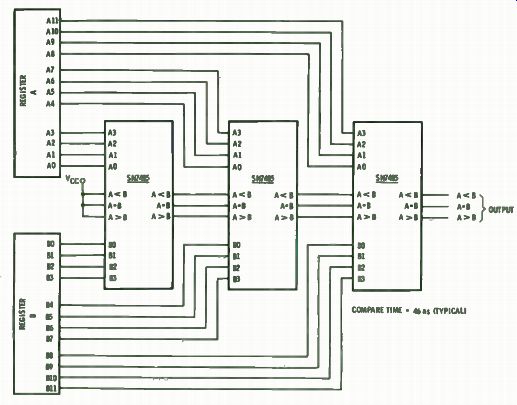
Fig. 7-11. Cascaded comparators.
When A3 = 0 and B3 = 1, Gate 1 goes to 1, Gate 2 goes to 1, Gate 3 goes to 0, and Gate 4 goes to 0. Again, Gates 6 through 15 are driven to a 0. Gate 5, however, is driven high while Gate 16 is driven low. Thus, the A < B output goes high while A > B goes low; Gate 19 is also low.
When A3 = B3 = 1, Gate 1 goes to 0, which drives Gates 2 and 3 to 0 and causes Gate 4 to go high. Gates 6 through 15 plus Gate 19 are now free to follow their other inputs. Gates 5 and 16 are driven low, which allows Gates 17 and 18 to follow their other inputs. When A3 = B3 = 0, Gate 1 goes high, but Gates 2 and 3 are held to 0 by their second input and Gate 4 is high. The same output states are obtained.
When A3 = B3, the state of the outputs is determined by A2 and B2 in a similar manner. If A2 and B2 are also equal, outputs are determined by A1 and B1, and then by A0 and B0. When all bits are equal, Gate 19 is satisfied and goes high.
For words longer than 4-bits, comparisons can be made as shown in Fig. 7-11. In this case, the signals for the A < B, A = B, and A > B inputs are obtained from the preceding stages. These cascaded inputs allow a "tree" of comparators to operate as a single, large comparator.
Prev: Link | --Link | --Link | --Link | --COUNTERS
Next: PARITY AND PRIORITY
Guide Index : Transistor-Transistor Logic (early 1970s)