
by Gerald Stanley, Research and Resources Manager, Crown International, Elkhart, Indiana
One of the major problems of solid-state amplifier design has been the protection of the power-handling output semi conductors. Amplifier output stages generally experience the greatest stress of any part of the design and at the same time represent the section of the amplifier most likely to employ new semiconductor technology or new design ideas. This combination of stress and relatively new hardware has produced more than one product that performed faultlessly on the test bench but defaulted in regular use. This has been especially true in the professional sound market where the performance demands are sustained at a higher level and operating conditions are less forgiving of any design shortcoming.
The last ten years have seen various designs in tended to solve the fundamental problem, excessive localized heat in the output transistors. This leads to a regenerative destruction mechanism known as second-breakdown. Power transistors have been placed in parallel or in series to spread the dissipation over more devices, and various forms of voltage and current limiting have been added to the mix to limit the possibility of damage. In some cases, all protection attempts have been abandoned except for relatively slow and indiscriminate circuit breakers or fuses. The idea was to save cost and reduce distortion resulting from operation of limiting circuits. An analogy might be drawn between this approach and that of selling a car with no brakes be cause of the expense and waste of energy that results from an adequate braking system.
The function of the protection system is to prevent total distortion, that is, amplifier failure. The most popular design is the V-I (voltage-current) limiter and its many variants. Such a design is shown in Fig. 1. In order to understand the kinds of problems faced by designers, it is worth a look at the V-I limiter to understand its strengths and weaknesses.
Such limiters were first developed to protect series-regulator power supplies and soon thereafter were used in amplifiers. They all use the resulting summation of a signal proportional to Vce (the output transistors' collector-to-emitter voltage) and a signal proportional to Ic (the output transistors' collector current) to limit the drive signal to the output devices. Either signal may be constructed with a nonlinear network, such as a resistor-diode network, to improve the fit of the allowed locus of stress to the transistor ratings as revealed by a safe-operating-area or SOA plot. Such an SOA plot is shown in Fig. 2 for a single transistor of the type being considered.
As shown, the SOA is valid only for a rectangular pulse of the noted duration and if the case temperature is held at a constant 25 degrees centigrade. A typical protection area for the circuit of Fig. 1 is drawn in dotted lines in Fig. 2. Since it is unlikely that a heat sink can be devised that will maintain the case temperature at 25 degrees under all conditions, it is generally decided to derate the limiter design. The derating pro cess takes into consideration the maximum possible case temperature as bounded by a thermally activated cutout switch. Since the indicated circuit does not respond directly to Vce but rather indirectly by assuming a nominal supply voltage (not necessarily disregarding regulation), it will also be necessary to consider maximum line voltage effects when choosing the derating for the limiter design. (The latter effect may be eliminated by using a different Vce sensing network and/or altering the control topology of the circuit, but the possibility is not shown in Fig. 1, which is the most typical circuit.)
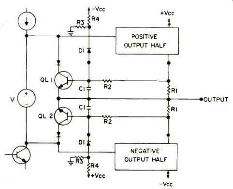
Fig. 1--Typical V-I limiter circuit.
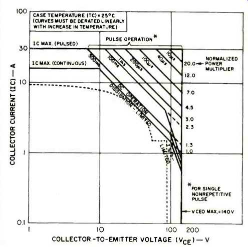
Fig. 2--A typical SOA plot.
The circuit also does not fully appreciate the history of the signal and, as such, cannot take advantage of the shorter time interval pulse boundaries of the SOA surface shown as a family of curves in Fig. 2. This constitutes the greatest deficiency of the V-I limiter because it does not allow the maximum possible output from the output devices at all times. If the V-I limiter is designed around one of the shorter-time interval boundaries, the amplifier will surely fail in use since long time interval stresses routinely occur when overload or low-frequency inputs are present. The use of transformer or auto-transformer coupling to loads can exacerbate such trouble, as can ultrasonic system oscillations.
The typical extension made to the V-I limiter involves the use of a capacitor as a simple lowpass filter of the signal which controls the limiter. C1 of Fig. 1 is such a capacitor.
This presumes that the thermal circuit of the output devices can be modeled as a single RC circuit, as is shown in many elementary texts on semiconductor device heat sinking. A little examination of real-world data quickly reveals this assumption to be false. Figure 3 is a curve showing the relation of thermal resistance to pulse length for the case of a rectangular pulse of power. The plot of a simple RC network is shown (dotted line) for comparison. The more proper electrical circuit for simulation of thermal impedance would be either an RC low-pass ladder network or its series RC equivalent as shown in Figs. 4A and 4B respectively.
The use of C1 also assumes that the control signal charging C1 is a signal representative of the power stress on the semi conductor device which is, of course, a function not of the sums of voltage and current but the product of voltage and current. The control signal, if properly constructed, must in corporate a multiplier! In essence, if a protection circuit is to allow a maximum of instantaneous unlimited output (certainly of critical importance when music signals make up the primary signal source), it must take into consideration the complexities of the actual time-temperature behavior of the semiconductor junction. While the V-I limiter may be further elaborated to increase its conformity to these goals, it is cumbersome at best to proceed along these lines. As an additional consideration, temperature dependence of the heat sink must also be fully integrated with the circuit function, if the last safely available output watt is to be obtained. A worthy objective from many a user's point of view would be to eliminate total shut-down in the case of high sink temperatures, in favor of automatically derated output.
Assuming that semiconductor devices are available for use that are not prematurely derated by high voltage to values of power dissipation less than those obtainable at low values of Vice, an ideal protection system might appear as diagrammed in Fig. 5.
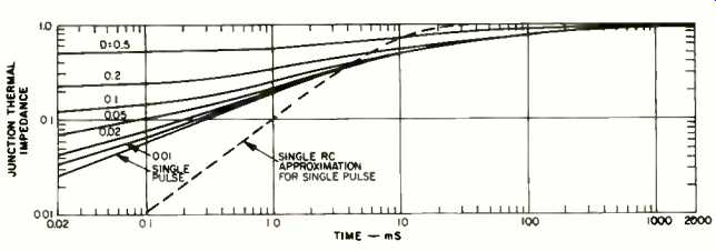
Fig. 3--Junction thermal impedance vs. time.

Fig. 4A--Electrical analog of thermal impedance.
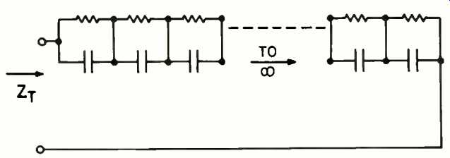
Fig. 4B--Series RC equivalent of 4A.
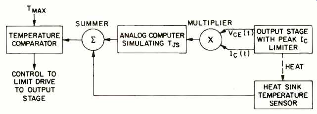
Fig. 5--Proposed protection system.
The topologies of some output stages are shown in Figs. 6A-6C. Figure 6A is the most common, the "totem-pole" output stage. Figure 6B is the full bridge which is used in high-reliability very-high-power designs, such as our Crown Mod el M-600. Resembling 6A, Fig. 6C is a variant of the totem-pole which is proposed for reasons which will become obvious. The relationship of 6C to 6B is that it constitutes the "lower-half" (left-hand side in 6B) of the full bridge as op posed to the "upper-half" (right-hand side in 6B) that constitutes Fig. 6A.
Two protection systems (per channel) must be fabricated in an actual power amplifier since there is a minimum of two such power stages that require protection. This poses some practical problems regarding complexity which can not only make the cost prohibitive but may also damage the unit's reliability due to the greatly increased parts count. If this system were deployed in the typical design, it would most readily be done by sensing the output current common to the output terminal of the topology shown in Fig. 6A. This would require the addition of supplies common to the output terminal if we wish to allow the use of IC op-amps in the construction of the protection systems.
Since the control of the output stage may be accomplished by low-voltage drive circuitry which is common to ground, the topology of Fig. 6C is much to be desired for the implementation of the desired protection system. As such, not only may the same supplies that drive the voltage amplifiers be used to power the protection circuitry, but also the circuitry may be easily observed for trouble-shooting and the high-voltage output circuitry may be driven by low-voltage drive amplifiers. In what may come as a surprising result, the nature of the output open-loop impedance and gain is not materially altered by this change since both topologies are typically driven by a current source and degenerated by an input capacitance which connects the output stage input to the d.c. supplies of the output stages. The construction of a special set of low-voltage common-to-ground supplies for the controlling circuitry is also useful when the addition of signal-processing add-on accessories are required.
The fact that the main power supplies cannot be common in a two-channel amplifier using the output circuit of Fig. 6C does not pose a serious problem. In an amplifier large enough for such a protective system to offer cost benefits, the weight of the power supply should be well distributed, and in fact the use of two main power transformers is cost effective in terms of chassis structure costs.
The design of the junction-temperature-simulation protection circuitry poses major problems, primarily in acquiring device thermal parameters which are not found on data sheets. To make matters worse, it is not enough to have typical data since the worst case must be covered. Ideally one could calculate the thermal impedance vs. time from a few physical device parameters. This proves to be easier said than done, for variables such as imperfect conformity between device package and mounting surface are not readily analyzed.
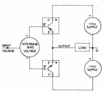
Fig. 6A--Totem pole output stage.
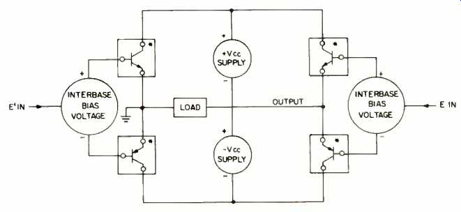
Fig. 6B--Full bridge output stage, as in Crown M-600.
The method used to observe the needed thermal characteristics called for observation of the temperature dependent voltage (Vcb) of the forward-biased collector-base junction during the cool-down phase following the application of a controlled pulse of power. The heat sink used was fully and accurately represented with all associated heat sources and temperature sensors exactly as they were to be deployed in the final amplifier. The use of the cool-down phase, rather than the heat-up phase, for analysis is dictated by the practical constraints of data availability. Cool-down is equivalent to the input of a step of negative power.
The capabilities for thermal analysis were incorporated into a third-generation nondestructive power transistor SOA analyzer, which upon command will produce the needed power stimulus and cool-down temperature data. Such a custom analyzer was developed after considerable experience in using units of earlier design for 100 percent quality control testing of all output devices used in our amplifiers.
The temperature data must be gathered over a large range of time intervals with rapid sampling being required immediately at the close of the power cycle, and infrequent sampling being required after a number of seconds have elapsed.
The use of sampling intervals that are nearly uniformly spaced on a logarithmic time scale represents a reasonable tactic for optimizing the amount of data needed to characterize a given transistor. Such a data gathering strategy requires the use of a computer-driven data acquisition system if the data is to be gathered in one pass. Since a large number of transistors is to be tested, this is mandatory.
The heat-sink temperature vs. time is also digitized and used to deduce the thermal circuit that lies between the heat-sink temperature sensor and the transistor junctions by differencing the junction and sink temperatures. The analyzer auto-zeroed itself at the start of each test to remove device-to-device differences in the 25-degree value of Vcb.
The data gathered from each device was captured in re cords in the computer's disc data files for reduction at a later date. This allows any desired algorithm for determining worst-case behavior or studies of the statistics of thermal impedance to be made as desired.
The method chosen for worst-case study of the data required the construction of a pseudo-device that represented the hottest temperatures seen at any given instant in time.
This did not necessarily result in just one device governing the worst-case model. The computer proceeded to find the characteristic values of the RCs used in the model of Fig. 4B.
This task is only suitable for a computer algorithm as no direct solution method is known for determining the coefficients, much less for hand calculation (which would take many man-years).
It was found that a three RC network gave an excellent fit to the data with an accuracy greater than the components to be used would actually produce. There was therefore no ad vantage in using four or more RC sections to simulate the junction behavior.
The resulting circuitry of the protection system is a two-quadrant multiplier which computes the product of Ic and Vce and is implemented with a monolithic transistor pair and op-amp current mirror. The single-ended output of the mirror is mixed with the output of a temperature-sensitive IC whose current output is proportional to absolute temperature.
The protection circuit's temperature computer is composed of an inverting IC op-amp with the determined RC impedance analog networks in the feedback loop. The virtual ground input receives the instantaneous power signal from the multiplier as well as the signal from the thermal sensor.
As configured, a single quad-pack op-amp suffices to con struct the protection circuit along with two monolithic dual transistors and two IC heat-sink temperature sensors. Since the output stage is built with one heat-sink module per output stage half, no interstage interaction interferes with the analysis. The circuit design is such that the protection circuit saturates at low junction temperatures, i.e. below 25 degrees centigrade. This is in conformity with the device power de-rating being confined to the region of 25 to 200 degrees.
Another parameter which must be honored on the transistor's data sheet is the maximum d.c. collector current. To this end, a conventional diode drive-limiting network is employed. Failure to honor this specification will result in emitter lead-bond failure. Limiting collector current implicitly prevents exceeding the maximum d.c. base current. The instantaneous limiting of collector current also prevents any possibility of large amounts of dissipation occurring in very short time intervals (microseconds) which would not be accurately analyzed by the simulator, thus assuring the validity of the simulation.
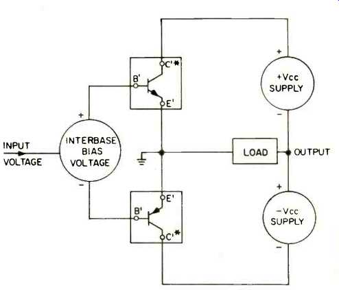
Fig. 6C--Modified totem pole.
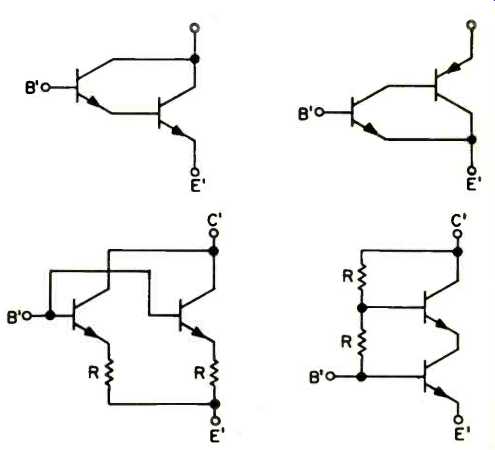
Fig. 6D--The composite transistors, marked with an asterisk in Figs. 6A-6C,
use any combination of the above.

Fig. 7--Schematic of the actual protection system.
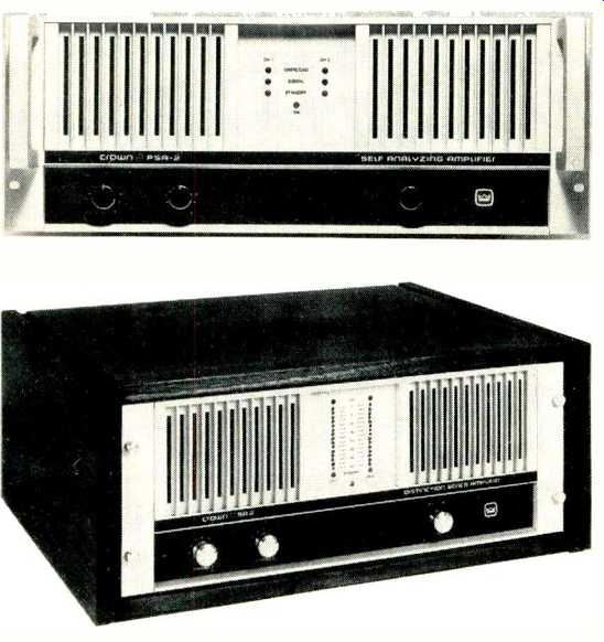
Fig. 8--Two Crown amplifiers, PSA-2 and SA-2, which incorporate the protection
system.
Views of the two amplifiers incorporating this design are shown. Both amplifiers share the following features. The rear panel has slide switches for engaging low-frequency protection to protect drivers from inadvertent d.c. or subsonic exposure. The detection of d.c. will then result in disabling of the main power supplies via relay control. This is a much more reliable system than a relay disconnect of the load which may not successfully break an inductive circuit having d.c. excitation. (The relay may weld with the arc!) The front panel display of the PSA-2 contains seven LEDs. An orange power indicator with channel independent yellow main power supply standby indicators shows if the supplies have been disabled. The supplies may be disabled for several causes such as turn-on delay, low-frequency output load protection, or transformer overheating. Two green LEDs indicate the presence of reasonable signal levels short of over load. Upon overload of any form--clipping, slew-induced, or protection circuit induced--the Crown-developed IOC indicators (red LEDs) will light rather than the green signal LED in the overdriven channel.
The front panel display of the SA-2 has two 15 LED (green) Jacob's ladder type displays in place of the two green signal-present LEDs of the PSA-2 display. One LED on each display indicates the current value of the peak signal, which another indicates the recent largest peak value of the signal for that channel. This display may be optionally ordered on the PSA 2 amplifier.
The incorporation of modern data gathering and numerical methods have made possible the design of power amplifier protection circuitry that was previously impractical. Such de signs are capable of withstanding torture tests (which represent real-world stress conditions), with a high degree of confidence of survival. This has been achieved with a subsequent enlargement in the undistorted audio output as compared with previous means of reliable protection.
To make maximum use of the concept, a new variant of the "totem-pole" output stage was deployed with consider able improvement in the observability of the amplifier output stage parameters. In short, a new generation of "solid" solid-state amplifiers has arrived that contains four analog computers which are the stepchildren of a digital computer's analysis of the output transistors.
(adapted from Audio magazine, Feb. 1981)
Also see:
Build a Class-A Amplifier (by Nelson Pass) (Feb. 1977)
Construct a Wide Bandwidth Preamplifier (Feb. 1977)
Transient IM Distortion in Power Amplifiers (Feb. 1975)
Trends for the Future (April 1980)
Build a Double-Barreled Amplifier--Part 1 (Apr. 1980)
= = = =