So much has been written and re-written about the chroma section in color television receivers that we felt compelled to avoid complicated, involved explanations in favor of a very simple, straightforward presentation that should stand the test of time. And after you have explored the block diagram, diode, transistor, and then integrated circuit demodulation, along with general color processing, you should have a very thorough idea of most, if not all the methods in use today and the many reasons for their existence. We begin with a block diagram, and then examine each section individually.
THE CHROMA SUBSYSTEM
There are three inputs to any U.S. chroma subsystem (Fig. 12-1). No. 1 is the chroma input from the first or second video amplifier. No. 2 is the burst, which comes from either the first bandpass amplifier or directly from the video amplifier, depending on the amplification needed. And No. 3 is the high-voltage transformer-generated gating pulse that turns the burst amplifier on.
Following the burst amplifier, there are often two comparators, each usually composed of a pair of diodes. They match the phase of the incoming color sync burst against feedback from the 3.579,545-MHz subcarrier oscillator, and correct the oscillator frequency. Also, there is a second comparator, doing the same thing as the first comparator, but this one generates a DC automatic control voltage, reputedly a linear function of incoming burst amplitude, that is supposed to proportionately regulate the amplitude swing of the band pass amplifier (s). The bandpass circuits, naturally, have a chroma amplitude control, while others also have a tint or hue control.
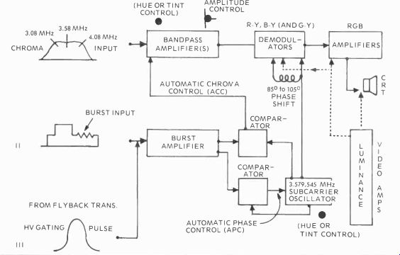
Fig. 12-1. Block diagram of the chroma subsystem bond in any U.S. made color
receiver. The arrows point in the direction of signal flow.
Fig. 12-2. Examples of the phase-shifting network used to divide the phase
of the subcarrier oscillator inputs to the R-Y and B-Y demodulators. Network
B) is the equivalent of A), and C) is the graphic analysis of either. Vertical
line symbols before 390 ohms mean parallel. The resulting phase angle difference
between Z1 and Z2 is 85 degrees.
The burst amplifier is gated into conduction by a comparatively large pulse from the flyback transformer every 63.5 microseconds for a period of between 5 and 10 microseconds to admit the color sync burst. This burst amounts to 8 to 11 cycles on the back porch of the horizontal sync pulse and on top of the blanking pedestal. There may be a hue or tint control that manually governs the phase of the 3,579,545-MHz subcarrier, rather than the one bracketed in the bandpass amplifier; this is a choice among the various manufacturers, but usually the phase of the subcarrier is shifted since it's a simple sine wave and easier to control.
The bandpass information now goes to the demodulators.
Also applied to the demodulators are two subcarrier oscillator signals, one at 85 degrees and the other at 105 degrees from burst. These phase angle separations are, however, entirely predictable, either by straight math or through a relatively simple system of graphic circuit analysis that we'll demonstrate. The circuit, along with its analysis, are both shown in Fig. 12-2. Initially, we see a 180-pf capacitor in parallel with a 390-ohm resistor. The 390-ohm and 330-ohm resistors (in series) are paralleled with a 150-ohm resistor. Finally, there's the 10 microhenry series coil in the Z2 output.
First, let's show the sum of the 150- and 330-ohm resistors on the graph-no phase shift. We'll drop a perpendicular from the 330-ohm resistor to some convenient point, cross over to the Y axis, then draw a line from 0 X-Y to the right corner of the diagram and another line from the parallel ( ) 390-ohm resistor to the left lower corner in the third intersection.
Where the three junctions meet, and directly up to the X axis, is the resistive (RT) total. Now, we calculate the reactance of the 180-pf capacitor:
Xc = 1/2Trfc and this amounts to 247 ohms, which is promptly measured on the 4th quadrant negative Y axis. A line is drawn between this point and RT, and a perpendicular laid off to the 0 X-Y junction on the left. This angle, measured by protractor, is-40 degrees.
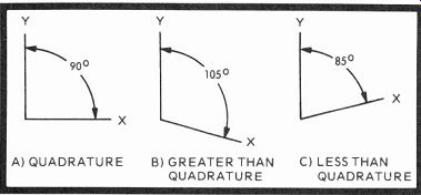
Fig. 12-3. Angles of demodulation used in the past and present to drive R-Y,
B-Y and sometimes G-Y, although G-Y is always a function of the reds and blues.
A) quadrature was Zenith's original; B) now the phase angle used by almost
everybody; C) RCA's most copied X and Z original.
The inductive reactance:
XL = 2TrfL is calculated at 224 ohms, and, because it is inductive, is laid off vertically according to the measured distance, and a diagonal is again drawn to the 0 X-Y axis. The measured angle here is 45 degrees. So, from-40 to +45 is an algebraic total of 85 degrees, and this is the same type of phase angle shift we show accomplished by a simple coil in Fig. 12-1.
With an adequate vectorscope, you would see this phase angle precisely reflected in the vector output as the phase difference between the third R-Y and sixth B-Y vector petals (Fig. 12-3). At 85 degrees, this angle would be less than quadrature, while at 90 to 105 degrees it would be equal to or greater than quadrature. These phase angles are determined at times by some of the "company official viewers," while at other times-and this is the more prevalent condition now, thank goodness-by the design engineers who are trying to find the best angle to complement the latest RGB phosphors.
With yttrium phosphor reds, the usual angle of demodulation is very nearly 105 degrees. Green now, however, is the weakest phosphor, and so the newest receivers "key" on this color instead of red, as most did in the older tubes when blue and green were the stronger phosphors.
The "demodulator evolution" began with RCA's X and Z type, which demodulated at an angle less than 90 degrees and used relatively few components. Some off shore and USA manufacturers continue their use even today. Next were Zenith's original high-level demodulators, which amplified first (the opposite of the RCA system) then demodulated, passing the demodulated chroma directly to the electrodes of the picture tubes. Both these systems, by the way, fed the color signals to the grids of the picture tube (Fig. 12-4) and luminance into the cathodes; the picture tube actually did the RGB and Y matrixing (mixing). Both these systems derive the greens from negative portions of the R-Y and B-Y inputs (Fig. 12-5A through E). The second innovation (B) used principally by Motorola and RCA, was the 3-diode matrix, where G-Y was actually demodulated separately, but RCA still went to the cathodes and grids, while Motorola put pure RGB directly into the CRT cathodes and grounded the grids at the AC level.
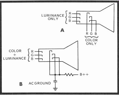
Fig. 12-4. Old style separate chroma and luminance CRT inputs (A) to the
grids and cathodes. In the newer version, all drive signals go to cathodes
of the CRT, with control grids at AC ground (B).
Next, Motorola (C) put chroma and luminance together into an integrated circuit, and went into the CRT with pure RGB. At about the same time, Zenith (D) began demodulating R-Y and B-Y with an IC, matrixing the Y and greens, then amplifying before application to the cathodes of the CRT.
Finally, in 1970, RCA and Zenith "IC'd" (E) the entire chroma and subcarrier color sections, and fired the CRT cathodes directly with reds, blues, and greens.
The reason for going to cathode CRT operation, according to Fairchild's Normal Doyle, is that with the tube matrix system, gray-scale tracking adjustments are made in the luminance channel. And this requires qualification in the demodulation process because of the difference in phosphor efficiencies and to relate the grid drive more nearly to the cathode drive. In the red, blue, green system (RGB), however, color-difference signals are mixed before entering the CRT, and only the cathodes are driven, while the grids are at AC ground. In this method, both signals are already arriving at the same set of tube electrodes simultaneously; therefore, no individual correction is needed for best color reproduction.
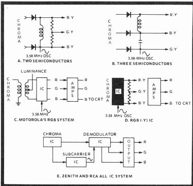
Fig. 12-5. Chroma demodulators in their order of development between 1955
and 1972. C and D were developed simultaneously. Actually, there's not an
enormous difference between the two latter systems.
MODULATION TO DEMODULATION
Although we talked about this subject somewhat in Section 1, more detail is needed so you will be able to trans late between the two with ease and certainty.
Since we cannot transmit two separately modulated subcarriers of different frequencies because of non-frequency interlace and the resulting beat that would ensue, we resort to two-phase modulation of a single carrier. These "two" sub carriers are of identical 3,579,545-Hz frequencies but are separated in phase by 90 degrees. In reality, just as in the receiver, this is actually a single carrier generated by a single source, with its slave branch phase-shifted 90 degrees.
Fidelity of color transmission and reception can be greatly affected by crosstalk among all the primary colors if the transmitted phase separation is not carefully maintained, and if the receiver is poorly designed or has component defects. If, for instance, there is carrier imbalance, a gray or white picture area will not cause the transmitted I and Q signals to go to zero, and these neutral shades become colored and are quite objectionable. Also, if there is a video unbalance, un desirable video will be added to luminance and distort the gray scale. A positive upset in the Q modulator, for example, would somewhat intensify reds and blues but darken greens.
Negative unbalances would intensify greens but shade blues and reds.
Transmitted signals start out, of course, as red, blue, and green information from the three picture tubes in the camera.
The three signals are channeled into an encoder or transmitter matrix, and come out as luminance, I, and Q intelligence.
These I and Q signals are each then put into a balanced modulator driven by the 3.58-MHz subcarrier oscillator (Fig. 12-6). The subcarrier is virtually suppressed during trans mission and, along with burst, luminance, and sync, go to the transmitter for external broadcast. Greens are included in both I and Q, so no separate green signal is transmitted.
The modulation and demodulation processes are illustrated by a diagram from Sylvania's Color TV Clinic Manual, Volume 1, by Eugene Nanni and his staff at GTE Sylvania, Batavia, New York. We've made a couple of changes, however, to suit our immediate purposes. See Fig. 12-7. As I and Q information reaches the transmitter diodes, the 3.58-MHz subcarrier makes each conduct in the peak signal sequence, turning one diode off while the other is on-a time sharing process called synchronous detection so that both signals may be placed on a single carrier. While in the receiver, the I and Q signals are initially phase shifted 33 degrees by the receiver circuitry, and R-Y, B-Y ( and G-Y in late receivers) is demodulated by an internally generated but burst sync'd 3.58-MHz oscillator to produce the same picture tones (phase and amplitude) of the transmitted signals. There are a number of ways to generate such synchronous demodulation which we cover shortly in the discussion of various receiver demodulator techniques.
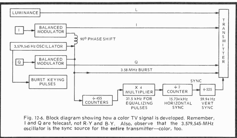
Fig. 12-6. Block diagram showing how a color TV signal is developed. Remember,
I and Q are telecast, not R-Y and B-Y. Also, observe that the 3.579,545-MHz
oscillator is the sync source for the entire transmitter-color, too.
Meanwhile, you should remember that chroma modulation is placing I and Q sidebands on two 90-degree out-of-phase suppressed carriers, removing luminance and transmitting video and color separately but on the same carrier. Conversely, demodulation is synchronous chroma sampling plus adding the luminance back to the chroma in formation by matrixing so there is brightness, including fine detail, in all color scenes. Recall that in monochrome reception there are no I and Q signals processed and luminance only is distributed usually to the cathodes of the CRT, with just DC bias to the control grids. When chroma is transmitted, you need to recall that the I intelligence includes colors ranging from bluish-green (cyan; to orange, while the Q channel produces colors from yellowish-green to purple (magenta) ). Again, the bandwidth of the I signal is 1.5 MHz and the Q channel is 0.5 MHz. But the receiver's bandpass is such that it can demodulate color only to 0.5 MHz, whether R-Y or B-Y, and this is why the incoming chroma appears as a 1-MHz passband (3.08 to 4.08 MHz) across the 3.58-MHz reconstituted subcarrier (Fig. 12-1).
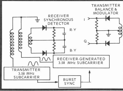
Fig. 12-7. Simplified modulation and demodulation diagram with subcarrier "sampling" diodes
to produce colors at the conduction peaks. The transmitter 3.58-MHz oscillator
syncs the receiver subcarrier oscillator by the sync burst.
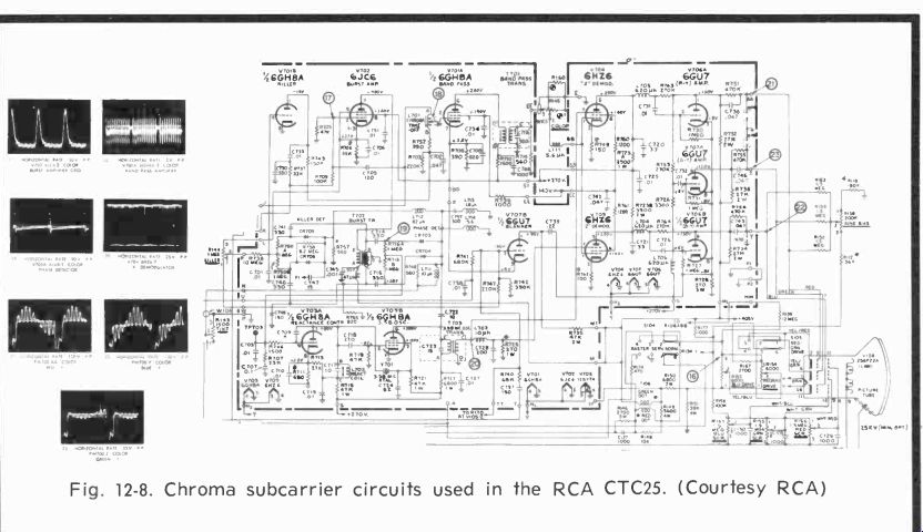
Fig. 12-8. Chroma subcarrier circuits used in the RCA CTC25. (Courtesy RCA)
RCA'S CTC25 CHROMA CIRCUITS
In this mid- '60s vacuum tube receiver (Fig. 12-8) chroma is applied to the bandpass amplifier through terminal J, while terminal K carries the flyback turn-on pulse for the burst amplifier. With no incoming chroma, the potential at the V707B blanker grid is-90 volts, much of which finds its way to terminal 1 of the R144 1-meg color killer potentiometer, while the top of this control, pin 3, sees +27 volts at the cathode and suppressor of the burst amplifier, showing that this tube is conducting because of the continuous flyback pulse. With no incoming color, the killer control is adjusted so that it just cuts the color killer on, delivering negative DC to the grid of the bandpass amplifier, cutting the tube off. With a chroma input, however, color sync reaches the burst amplifier through C705, and turning on the burst amplifier feeds burst transformer T702. The transformer output goes first to voltage-phase comparator diodes CR705 and CR706, which generate a varying control voltage to turn off the color killer so that its plate becomes zero, and permits the bandpass amplifier to receive chroma at its grid through chroma takeoff coil L701.
At the same secondary of the burst transformer are two more phase detector diodes, CR703 and CR704, that compare the phase of the 3.58-MHz oscillator with the phase of the in coming burst. The DC correction varies the grid voltage on reactance control V703A. This tube looks like a capacitor to crystal-controlled 3.58-MHz oscillator V703B, and so holds the oscillator in sync with the transmitted color sync burst by speeding up or slowing down the oscillator. Signals from the 3.58-MHz sine-wave oscillator go to pentode X and Z demodulator suppressors (the phase of the signal to V709 is shifted 90 degrees). In-phase chroma signals go to the V704-V709 grids. The two tubes conduct on the positive sine-wave tips, producing R-Y and B-Y outputs that differ in phase by less than 90 degrees. Green is resistively derived in the G-Y amplifier through the voltage divider between the X and Z demodulators and 270-ohm common cathode bias resistor R728. Chroma is then amplified and coupled by capacitor-shunted resistors to the CRT grids. Luminance is applied simultaneously to the tube's cathodes because of the 0.8 microsecond delay line between the second and third video amplifiers.
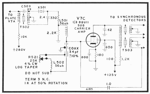
Fig. 12-9. General Electric's 3.58-MHz crystal ringing circuit. (Courtesy
Bob Hannum)
Arriving through PW700 terminal T is a large positive blanking pulse that drives the V707B blanker into inversion and produces a negative blanking pulse every 52.4 microseconds for some 11.1 microseconds duration, which turns off the three color amplifiers. In Fig. 12-8 the color amplifiers are passing a color-bar generated pattern which shows large negative off periods, with considerable variation in AC color-bar amplitudes, depending on color signals reaching the RGB (-Y) outputs. The DC plate voltages with no incoming signal can be almost identical.
In operation, the blue gun is conducting the hardest, with red second, and green only a few volts, since we might assume the blanking pulse was included as part of the recorded waveforms, as it should be in the usual technician's evaluation. In engineering, we would mentally separate the two at once, since neither is a function of the other, and are completely separate entities. From the amplitudes of the various waveforms we could then deduce that blue was probably the weakest phosphor, followed by red, and then green.
GENERAL ELECTRIC'S CRYSTAL RINGING CHROMA OSCILLATOR
Another way to sync a chroma subcarrier oscillator is to use a high Q crystal filter (Fig. 12-9). This actually rings in damped sinusoids when "hit" by the color burst signal. Its advantage is that neither an automatic phase control (APC) nor a color killer circuit is required, since the crystal will not oscillate unless there is incoming color and, when excited, will directly provide all sync oscillations in the proper phase.
Although the subcarrier amplifier shown in Fig. 12-9 is a tube type, the ringing crystal works equally well with semiconductors.
R521 is the tint control that induces a vector-like RL phase shift in the grid of V7C so that the best fleshtones can be manually tuned. Feedback is applied through the 1-mfd capacitor from the negative lower winding of T503, while the 800- and 62-pf capacitors in the grid and plate circuits are stray oscillation-preventing filters. Notice that the screen grid resistor is only 100 ohms, while the plate supply from the same DC source is applied through a 1.2K resistor and the primary of T503. This keeps the output at a certain level and "limits" the output to a certain DC swing. The voltage drop across either the 100-ohm or 1.2K resistors divided by the values of these resistances will, of course, tell you the current drawn by each electrode.
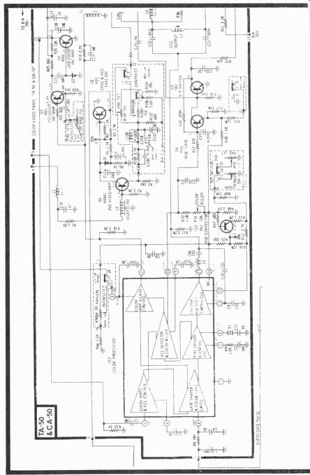
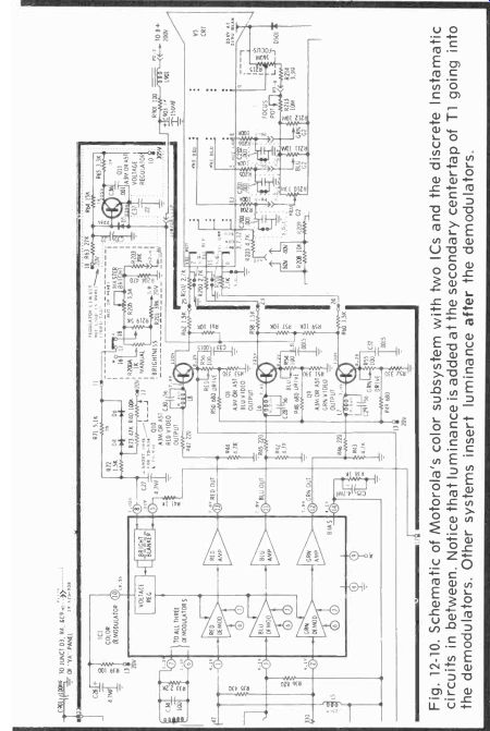
Fig. 12-10. Schematic of Motorola's color subsystem with two ICs and the
discrete Instamatic circuits in between. Notice that luminance is added at
the secondary centertap of T1 going into the demodulators. Other systems insert
luminance after the demodulators.
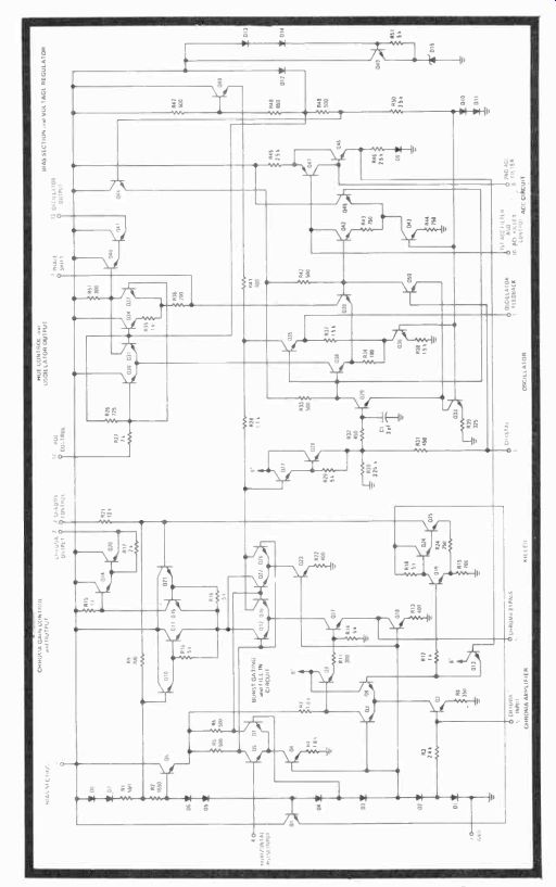
Fig. 12-11. Schematic of the Motorola MC1398 IC used in the CTV8 color processor.
(Courtesy Bill Slavik)
MOTOROLA'S DISCRETE & IC COLOR SUBSYSTEM
The Quasar CTV8 chassis (Fig. 12-10) contains an integrated circuit color processor (IC2) and an integrated color demodulator (IC1). IC2 is an MC1398 which provides DC control for both chroma amplitude and phase shift, a crystal- controlled feedback oscillator, built-in noise immunity, a Schmitt trigger color killer automatic chroma control, burst gate and pulse shaping, oscillator lock, and built-in voltage supply regulation.
A schematic of the MC1398 is shown in Fig. 12-11. Signal voltage for the color amplifiers and automatic chroma control functions comes from the emitter of the first video amplifier to pin 5, with a 0.05-mfd capacitor bypass at pin 6 (Fig. 12-10).
The chroma amplifier (Q2, Q3, Q8, Q9, Q17 and Q18) takes its DC references from the series diode regulator string and upper left regulator output transistor Q6. The chroma amplifier supplies inputs for the chroma gain and output section directly above. Transistor Q2 is a constant-current source, while Q13 is a bias and operating source for both the chroma amplifier and the color killer Schmitt trigger to the right of the amplifier. Differential amplifier Q3-Q9 supplies Q8 with in coming chroma that is emitter-coupled to the base of Q17, another amplifier which receives regulated emitter current by bypassed Q18. Output from inverter Q17 now goes to the emitters of Q12 and Q16, half of a dual differential, constant current fed (by Q23) Q22 and Q26 gated switch.
Gating for the differential amplifier (applied through Q5 and Q7) is switched by a 4-microsecond 3-volt p-p flyback pulse to pass the reference burst information used to lock the 3.58-MHz chroma oscillator. The second half of switched amplifier Q22-Q26 is used to prevent undesirable level changes in chroma during gating.
Outputs now go to chroma gain control differential output amplifier Q11-Q15 and the gating inputs Q10 and Q21. DC bias for both Q10 and Q21 is set by the chroma intensity control outside the IC by voltage division from the internal connection between R1 and R2. Therefore, the conduction of Q11-Q15 is controlled and Darlington output Q14 and Q20 provides a linear chroma signal at pin 2. Without incoming chroma, there is no bias from Q13 for the Schmitt trigger, so Q19 goes high while Q25 conducts hard, pulling the base of Q21 down and turning the transistor off so there is no noise or transient output.
The oscillator, of course, generates the 3.579,545-MHz chroma subcarrier, with a conventional crystal attached to pin 8. An RC series feedback network connects to ground from pin 1, a hue corrector and color killer control circuit at pin 10, and another capacitive filter at pin 9. Darlington pair Q27 and Q28 pick up the burst signals from Q16 and Q26 in the chroma amplifier section and deliver them to the base of the first section of the subcarrier oscillator, Q29. This transistor and Q50 form a differential pair from which the output level is proportional to that of the incoming burst. The conduction of each transistor then excites the rest of the Q35 through Q39 oscillator network. Oscillator output through Q38 goes to the emitters of Q30-Q31 so that hue control can be established. An oscillator signal also is applied to the emitters of a second differential pair, Q34 and Q37, for a 3.58-MHz output through Darlington pair Q40 and Q41 to pin 13-the oscillator signal exit for all three demodulators. The sine wave from Q39 is phase shifted somewhat by R36 and external capacitor C9. The hue control is simply another DC bias potentiometer that can manually change the bias on the two differential amplifiers which are already 180 degrees out of phase. DC bias changes mix the contents more or less and change the resulting output phase.
The automatic chroma control circuit supplies two operations: the first rectifies the subcarrier sine wave by differential offset amplifier Q42-Q45 and puts out a DC voltage proportional to the incoming chroma signal. The second function is adjustment of the operating point for Q46 and Q47 through the action of the controls at pin 10. With incoming chroma, the ACC output turns on the Schmitt trigger input, Q19, and turns off output Q25, which then has no affect on Q21 and Q15, but Q13 still supplies operating bias for Q9. With no ACC, naturally, Q19 is off, clamp Q25 is on, Q9 has no base bias and so ceases to conduct. Voltage regulation and bias drops are generated by Q48 and Q49 with D12 through D14 and reference zener D15, while D10 and D11 provide base bias for Q33, the current feed for Q29 and Q50.
Normal chroma out (Fig. 12-10) then passes through pin 2 to mixing transformer T1, while luminance information arrives the centertap in the T1 secondary, where both chroma and luminance are combined. But, remember, the chroma must be demodulated. The 3.58-MHz subcarrier sine-wave output appears at IC2 terminal 13 and is applied by way of RLC coupling to the red, blue, and green demodulators. In passage to the demodulators, however, the chroma in formation meets some unfamiliar passive and active components making up the "Instamatic" circuits.
There are two groups of circuits in the Instamatic: one, the variable potentiometer group which is preset and which controls the brightness, hue, contrast and intensity. An active semiconductor group increases the red output gain and monitors the amplitude of the second color "Int." amplifier and changes the demodulator phase. Transistors Q6 and Q7 act as an AND gate when the Instamatic is active, so that Q7 shunts the red drive control (R32) and allows more current to flow in the Q10 emitter, and therefore, the collector. As a result, Q10 conducts harder and supplies a slightly reddish tint to the CRT screen. At the same time, the 3.58-MHz phase angle to the blue demodulator is changed slightly through C21 and, together, the two changes cause the screen to broaden the area of fleshtones.
The other active part of the Instamatic circuit is com posed of color "Int." amplifier Q3 and Q4. A chroma signal applied to the base of Q3 where it is amplified, then the chroma goes through C15 and negative rectifying diode D2. This forms a relatively linear AC-to-DC feedback which controls the intensity of the color amplifier. The feedback is applied to pin 3 on the IC processor when the Instamatic switch is turned on.
Luminance information passes through delay line L2 to the base of the second video amplifier. Two video signals are taken from Q1, one from the collector for the noise limiter and emitter-follower sync and AGC gate, and the other goes from the emitter to a series peaking coil and RC video peaking to the secondary centertap of T1. A negative spike of voltage (noise) strong enough to turn on D1 causes the diode to shunt both the AGC and sync outputs to AC ground through C2. Limit adjust potentiometer R74 (not shown) sets the anode bias for D1.
MOTOROLA'S TRI-PHASE CHROMA DEMODULATOR
The chroma IC demodulator (no number as yet) is a thoroughly unique device in that it mixes luminance with the R-Y, B-Y, G-Y before demodulation. Pure RGB composite chroma and luminance are supplied to the final RGB amplifiers.
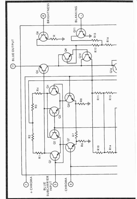
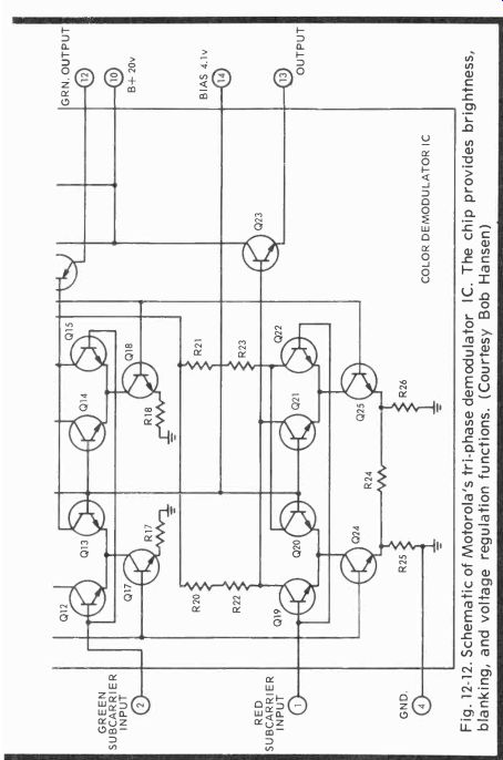
Fig. 12-12. Schematic of Motorola's tri-phase demodulator IC. The chip provides
brightness, blanking, and voltage regulation functions. (Courtesy Bob Hansen)
The circuit in Fig. 12-12 accepts combined luminance and un-demodulated color signals from T1 (pins 6 and 7) 180 degrees out of phase-for each of the red, blue, and green processors. The subcarrier sine wave is supplied directly from IC1 pin 13 by LC coupling to the three demodulators at the required phase relationship to produce properly phased outputs. The brightness control (R200A) sets the operating potential on the brightness-blanker stages that, together, control a pair of Darlington (Q9-Q10) current multipliers to supply collector voltage and current for the trio of virtually identical demodulators. The DC input is pin 10.
Positive chroma goes from the top winding of the T1 secondary through demodulator pin 7 to the base of Q8 (the driver-current supply for blue demodulators Q3 and Q4), to the base of Q18 ( the green drivers Q14 and Q15) and finally to Q25 (the keyer for red demodulators Q21 and Q22).
Negative chroma comes from the bottom of the Ti secondary, 180 degrees out of phase, and is supplied to the bases of current drivers Q7, Q17, and Q24 for the blue (Q1 and Q2), green (Q12 and Q13) and red (Q19 and Q20) demodulators, respectively. The DC bias for the bases of the differential amplifiers' synchronous switches already identified comes from the external 20-volt supply to Q2, Q3, Q13, Q14, Q20, Q21.
As positive and negative chroma signals are delivered to each of the current sources, the 3.58-MHz reconstituted sub-carrier sine wave (at controlled phase angles) reaches the demodulator bases through pins 3, 2, and 1, reading from top to bottom. Observe that the collectors of Q2 and Q4, Q12 and Q14, Q20 and Q22 are cross-coupled directly to an extra load resistor, since only one gate is operating at any given period.
Chroma signals (we discuss this more thoroughly in the next IC analysis) are applied positively and negatively to the six current driver supplies to keep the synchronous switches operating as the subcarrier sine wave tops cause conduction at externally set phase angles. In this way the individual switches conduct current through the various load resistors, developing voltages that are 7.16 MHz outputs.
Blanking transistor Q11 receives a flyback pulse from pin 5 that clamps it to ground and lowers the collector voltage supply through the Q9-Q10 Darlington pair for about 10 microseconds at the end of every line scan. This same Darlington pair also supplies voltage regulation for the switching transistors by stabilizing the B+ input at pin 10.
Capacitor shunted series inductors L6, L7 and L8 (Fig. 12-10) oppose any subcarrier voltages that might filter through, while the RGB drivers each have a DC current flow adjustment in the emitter. A diode-clamped single transistor regulator supplies collector voltage for the three RGB drivers. Individual color signal outputs go directly to the CRT cathodes.
ZENITH'S THREE-CHIP CHROMA PROCESSOR
For an idea of what these three chroma processors look like when mounted in their plug-in sockets, see Fig. 12-13. Fig. 12-14 is a schematic of the thick film resistor matrix interface between chroma and subcarrier regenerators. There are no transformers to twiddle in these chroma circuits, and only three DC pots that are quickly adjusted for complete chroma alignment. However, instead of simply eyeballing the adjustments with a color-bar pattern, we would recommend that the crosstalk adjustment be done with a vectorscope, too. You will see why later. Careful adjustment will allow maximum bandpass and chroma input amplitude-two essentials for quality color reproduction.
The uA780, 781, and uA746 (Fairchild designation) constitute an automatic phase control loop chroma processor in three monolithic integrated circuits that have a low phase error because of the high-sensitivity phase locked loop. The ICs are housed in 14 and 16-pin hermetically sealed ceramic packages for easy insertion and removal from commercial IC holders. In volume, all three collectively should be available this year (1972) for $2.
uA781C Chip
The 14-pin chroma processing chip is a uA781C Fairchild monolithic IF amplifier consisting of a pair of complex gain-controlled circuits (Fig. 12-15) in series, with the first designated as an automatic chroma control amplifier which receives all chroma inputs, but at all times is subject to DC ACC clamp from the uA780C IC chroma subcarrier regenerator. This amplifier is capacitively coupled to the chroma level amplifier, which, in turn, is clamped at its own DC swing by the chroma level control. Amplified chroma output goes to the uA746 third IC chip for color demodulation.
Between the ACC amplifier and the chroma level amplifier is a color killer switch with another DC killer adjust that tells this unit at what level to kill the chroma output. The actual ...
Fig. 12-13. Monolithic ICs in Zenith's 19CC19 and 25CC55 hybrid and solid-state
color chassis. These three chips do all the chroma processing, and are hand-removable
from their mounting sockets. (Courtesy Ed Polcen)
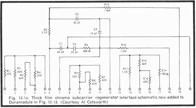
Fig. 12-14. Thick film chroma subcarrier regenerator interface schematic
now added to Duramodule in Fig. 12-13. (Courtesy Al Cotsworth)
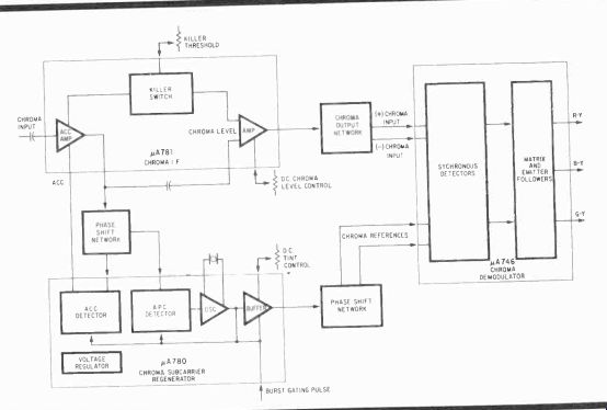
Fig. 12-15. IC manufacturer Fairchild's block diagram of the Zenith-developed
three-chip processor. (Courtesy Don Smith)
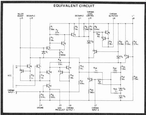
Fig. 12-16. Schematic of the uA781C chroma IF amplifier. (Courtesy Norman
Doyle)
...schematic for the uA781C chroma IF amplifier is shown in Fig. 12-16. ACC inputs are pins 1 and 14, which connect to emitter-follower Q11 and decouple stage Q8. Chroma comes in at pin 2 and goes to the base of Q10 for initial gain-control amplification.
DC voltages from the subcarrier regenerator are simultaneously applied to the automatic chroma control in puts. The potentials are different, however, and when Q8, for instance, is driven further into conduction to supply more base current to Q9 (which makes this emitter follower furnish more collector-emitter voltage for Q10 and Q12), the opposite phase voltage on Q11 causes this emitter follower to drive Q12 less.
As a result, the output of Q12 is regulated, as well as the output of follower Q14, the first chroma output shunted by switch Q13.
An opposite condition can occur, too, where Q11 can drive Q12 harder when there is less collector-emitter voltage from Q9.
Therefore, the gain-controlled chroma output at pin 6 is coupled to the input of the second chroma amplifier (Q15) at pin 7.
DC for the base of Q15 is regulated by zener diodes D4 and D5, which are supplied by Q7 from the power supply. D4 and D5 also furnish collector voltage and emitter-base bias for Q10, Q1, Q2, Q11, and Q8 in the stages just described and in the Q1, Q2, Q3 DC gain control circuits that monitor the DC from the level control relative to the potential at the collector of Q9 and the killer adjust. Diode D2 is a gain control, operating together with Q4 (like Q9 and Q12). Chroma from the collector of Q15 forward biases the emitter of Q4 and reaches the base of emitter follower Q6 as a positive-going signal identified at pin 9 as chroma output 2. Diode D3 supplies both bias and temperature compensation for amplifier Q4.
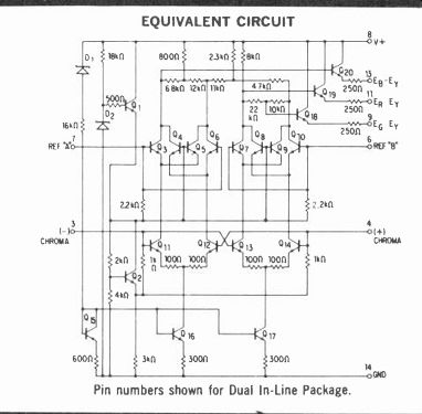
Fig. 12-17. Fairchild's uA746E synchronous demodulator IC schematic used
by Zenith. (Courtesy Frank Hadrick)
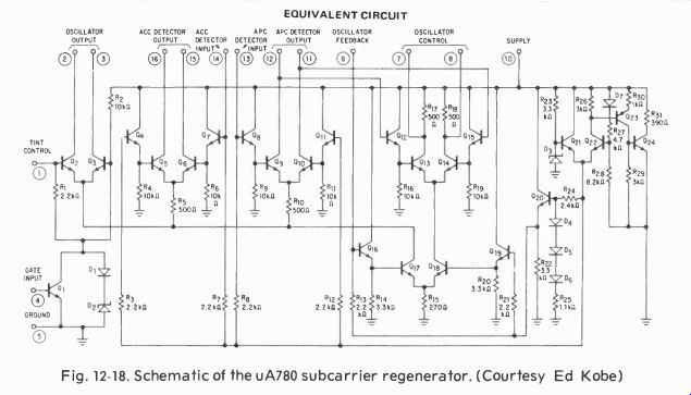
Fig. 12-18. Schematic of the uA780 subcarrier regenerator. (Courtesy Ed Kobe)
The block diagram says that the killer adjust affects both sets of chroma amplifiers, and indeed it does, for when there is no incoming color, and, therefore, no ACC input, Q8 and Q9 cease conduction, there is no chroma no. 1 output and, consequently, no chroma no. 2 input or output. Actually, Q1 and Q2 form a Schmitt trigger, and as long as Q1 is off, Q2 is on, and Q3 can't operate, since its base is pulled below turn on. While automatic chroma is incoming, Q1 and Q2 remain in this condition and the circuit continues in full operation. But when the "kill point" is reached, Q2 turns off, forward bias appears across R2, Q3 turns on, and all current in Q15 is shunted through D2 to AC ground. Consequently, the output circuit is completely cut off. Short circuit protection is provided by Q13 at pin 6 and Q5 across Q6 at pin 9, these being the chroma 1 and chroma 2 outputs, respectively.
uA746E Chip
The IC demodulator chip (Fig. 12-17) has 29 resistors, 20 transistors, and 2 zener diodes that, along with three diodes, supply ample regulation for the two pairs of differential amplifiers and the eight emitter cross-coupled demodulator switches. Depending on whether the cathode ray tube red phosphor is gadolinium or yttrium, these ICs, through the phase-shifted input networks, will demodulate at approximately 90 or 105 degrees, respectively. We say "approximately" because modern CRT phosphors are somewhat different from those originally specified by the NTSC, and even though efficiencies are now approaching relative equality, slightly varying phase and drive adjustments are still needed to produce the best fleshtones (and Kelvin temperatures) without seriously neglecting a desirably true chroma reproduction of the surrounding scenery.
The uA746E is a network of transistors and resistors formed on a single substrate (foundation) so that the entire chip is monolithic-that is, a single piece of silicon. Continuous wave (CW) 3.58-MHz signals from the regenerated subcarrier oscillator are fed into REF "A" and REF "B," while positive and negative chroma goes to the pair of differential amplifiers that key the eight switching transistors in the differential collectors. Since a CW sine wave is always present, it is the differential amplifiers that control the sequence of operation.
The conduction of the differential is proportional to the in coming chroma signals. This, in turn, determines the output of the synchronous demodulator switches above them.
If negative chroma information is arriving at terminal 3, it is coupled to the bases of Q11 and Q13, and if plus chroma information is received at terminal 4, it travels to the bases of Q14 and Q12. Depending on the amplitude, Q11 or Q12, and Q13 or Q14 conduct more or less, turning on partially or fully the associated switches. If Q11 and Q12 are in conduction, the emitters of Q3 and Q5 are enabled by Q11 and the emitters of Q4 and Q6 are turned on by Q12. The 3.58-MHz subcarrier sine wave, meanwhile, forward biases the bases of Q3 and Q6.
Since 3.58 MHz signals put to the bases of opposite, collector-coupled transistors 180 degrees out-of-phase, and at 7.16 MHz, the chroma from the differential amplifiers is demodulated, but the subcarrier signals are virtually can celled at the collectors of Q3 through Q6, thereby removing the need for extensive external filtering, except for an LC circuit following the output load resistors. The same sequence of operations is true for amplifiers Q13 and Q14, and switch demodulators Q7 through Q10.
The intelligence from these two pairs of double-balanced demodulators is matrixed resistively in the respective collector circuits, with the outputs going to Q20, the B-Y emitter follower, Q19, the R-Y emitter follower, and Q18, the G-Y emitter follower. Observe that the green follower tap-off is between the 22K and 10K collector resistors in the Q7 to Q10 switch group. The G-Y is derived by adding parts of the inverted B-Y and R-Y chroma inputs into Q13 and Q14.
Biasing for current sources Q16 and Q17, which feed the two pairs (Q11 through Q14) of differential amplifiers, is supplied through zener D1 through the 16K series resistor.
Diode-connected Q15 is fed by the same source. The Q15 emitter is above ground by 600 ohms. The bases of Q16 and Q17 are clamped by this regulated voltage and supply a constant current for the amplifiers. A 3-volt bias for the bases of differential amplifiers Q11 through Q14 originates from Q1, whose base is clamped at a fixed potential by zener D2.
Initially, the emitter voltage of Q1 is 6 volts, and this is applied to the bases of the eight switching transistors. A voltage divider, however, drops this value at the base of Q2 to the point where the emitter of Q2 supplies a 3-volt bias, which is shunted to the bases of Q11 and Q14 through 1K resistors to fix these potentials at a positive forward bias of slightly less than 3 volts.
uA780 Chip
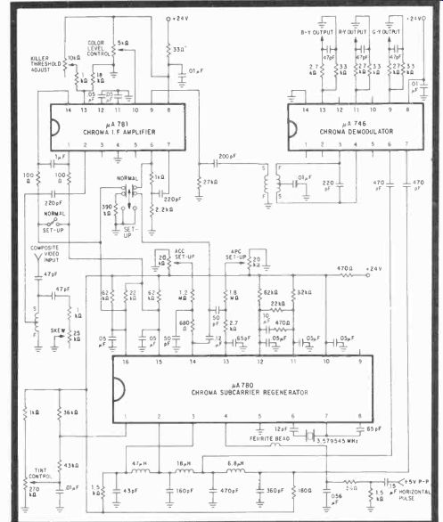
Fig. 12-19. Interconnection diagram for all three IC monolithic chips in
the complete Zenith chroma processor. (Courtesy Bill Edlund, Fairchild)
The uA780 phase locked loop subcarrier regenerator contains the 3.58-MHz oscillator that is phase-locked to the transmitter by burst through the automatic phase control detector. This IC also furnishes burst gating, DC tint, and automatic chroma control, plus its own regulated voltage supply. The schematic is shown in Fig. 12-18. An overall interconnection diagram for the entire chroma processor appears in Fig. 12-19.
The oscillator itself (pins 6, 7, and 8) is made up of two pairs of differential amplifiers, with bias and control gates at all inputs. Rigid control is provided by the APC detector DC outputs at pins 11 and 12. The oscillator, through feedback out of the base and emitter of Q16, drives the Q17 section of differential amplifier Q17-Q18 to supply the emitters of the APC and ACC detectors as well as the oscillator output at pins 2 and 3. The oscillator output signals are phase shifted by RLC components in the ladder network phase shifter and delay line where the sectional or total time delay can be calculated by N (the number of sections) times the square root of L and C:
written:
Td = NiLC
…while the output impedance is :
Zo = /ETC
This network is strikingly reminiscent of the DC delay lines used in radar for square wave pulses, but used here basically to separate the phase of the voltages going to pins 6 and 7 of the uA746 chroma demodulator by approximately 105 degrees.
APC and ACC setup controls are simple 20K potentiometers which are adjusted with the normal-setup switch in the setup position to provide bias at the bases of Q8 and Q7, respectively, without the benefit of incoming chroma. The subcarrier oscillator crystal is connected to pins 6, 7, and 8 (oscillator control), with feedback going to Q16 through pin 6 to complete the regenerative oscillator loop. Output from amplifier Q17 determines the phase for both the ACC and APC differential amplifiers, and makes one side conduct more than the other, depending on the respective DC biases during setup.
Each of the automatic correction circuits is heavily filtered at the appropriate output from the uA780 and so supplies relatively positive and negative DC correction voltages to both the oscillator (Q12 and Q15), as well as pin 1 of the uA781 chroma IF amplifier to control its gain. The gate input at pin 4 (Q1) is a blanking pulse from the horizontal output trans former, temperature compensated and shunted by diode D1 and protected by zener D2. A DC tint control voltage applied at pin 1 of the chip changes the Q2 bias, and so shifts the phase of the oscillator output.
Voltage regulation is achieved by the amplifiers and diodes in the upper right corner of Fig. 12-18. D3 is a reference zener for Q21, while D7 is a feed and temperature compensator for the base of Q22. Supply voltage changes will cause Q22 to conduct more or less, changing the base voltage of Q23 which conducts proportionately. As a result, Q24 varies the load on the 24-volt power supply, providing dynamic regulation for this portion of the chroma subsystem. D4 through D6 are also bias and temperature compensators for emitter follower Q20.
The three chips are manufactured at least by RCA and Fairchild, and perhaps others. RCA numbers for the Zenith system are: CA3070, CA3071, and CA3072.
RCA'S TWO-CHIP CHROMA PROCESSOR
The two-chip chroma processor for this receiver is shown in Fig. 12-20 with output connections to the MAD CRT driver modules that are the encapsulated thick film throwaways exhibited in Fig. 12-21. The MAC chroma 1 module is shown as a pair of "amplifiers" included in the A and B subsections of IC1, with outputs going to MAE chroma module 2, which has a voltage regulator governed by the output of pin 6, IC1B of chroma 1. All areas within the smaller dashed lines, of course, are on edge-connector plug boards, while the large dashed lines denote the mother board for each particular section. This series of RCA solid-state receivers has four mother boards, 12 plug-in modules, and a removable, single-piece high-voltage quadrupler.
We'll look first at the IC1 CA3066 (Figs. 12-22 and 12-23), that contains most of the color processors except the tint control and demodulators. Signals from the video preamplifier are coupled to pin 1 of the chroma amplifier. This stage, in which gain is automatically controlled by the ACC detector amplifier, supplies both the burst and bandpass amplifiers with signal. The chroma amplifier is stagger tuned to 4.3 MHz at pin 16 by the variable inductor and RC network, while the bandpass amplifier is tuned to 2.7 MHz, pin 13, by L2 and the RC combination so that the two combined can pass the 3.08- to 4.08-MHz chroma signals.
The subcarrier signal is introduced between pins 7 and 11 by a crystal ringing circuit. This type of oscillator control is a somewhat less expensive method of color sync than the phase comparator, and the neutralization and damping of the circuit must be carefully designed for best transient response, especially so that no hue shading appears after the vertical interval. On the other hand, with this type of circuit you could dispense with the color killer, but RCA didn't. You can drive the ACC with the 3.58-MHz oscillator, since the amplitude of the ringing signal is proportional to the amplitude of the burst, and a well-adjusted ringing circuit will lock on a single cycle of burst. The circuit also must be followed by a well-balanced demodulator, and it does need a color killer if automatic color control is a feature, which it is.
A horizontal keying pulse gates chroma from the band pass amplifier into the burst amplifier, and this stage, of course, rings the crystal for the 3.579,545-MHz subcarrier oscillator. Chroma gain is simply another potentiometer, as are the ACC adjust and color killer bias setting. Inductors L1 and L2 need alignment with a sweep generator for both band pass and gain.
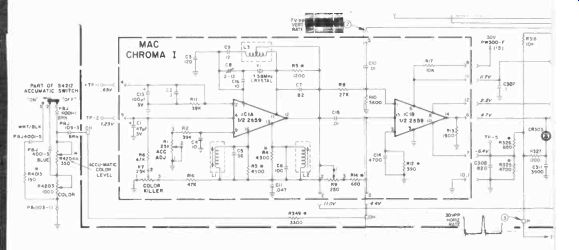
Fig. 12-20. RCA's sophisticated all solid-state CTC46 two- chip chroma processor
schematic. (Courtesy Tom Bradshaw, George Come)
Fig. 12-23 shows the schematic diagram of the IC1 color processor. Common-emitter and current source amplifier Q1 accepts chroma for collector coupling into the emitters of differential amplifier Q16 and Q2. The Q16 base is controlled by the amplitude of the 3.58-MHz oscillator through ACC action, and the output of Q2 is tuned by L1 and coupled through Z2 into the base of emitter-follower buffer Q19. This stage directly supplies Q3 and resistively controls the base of Q6 that, together, furnish current for differential amplifiers Q21-Q4 and Q7-Q24, the initial bandpass and burst amplifiers.
Burst keying appears at terminal 10 and is applied from emitter follower Q25 to the bases of Q7 and Q21 at a pulse width of 5 microseconds and 8 volts in amplitude. DC chroma gain adjust for Q20 and the bases of Q5-Q22, Q4 and Q24 is applied at terminal 15. Q5-Q22 is the final differential bandpass amplifier with its output at terminal 13, while Q7 is the burst amplifier output to L3, the crystal ringing transformer. The chroma bandpass amplifier is tuned by L2 and passed through zener Z6 to the chroma output at terminal 14, then to the demodulators.
Burst rings the crystal whose phase and frequency control the DC-coupled group of 3.58 MHz oscillator transistors connected to Q11 following terminal 7. The output of the sub-carrier oscillator goes to terminal 8 and also through the emitter of Q8 to the base of Q26. The oscillator is DC biased by ACC adjust R2. This is a loop gain adjustment where Q8 supplies current for the killer amplifier, in which the level is set by 47K R1, shunted by a 100-mfd capacitor. Q27 supplies DC for Q12 to keep it operating with the higher levels of the sub-carrier oscillator, so that Q13's base is receiving little or no voltage and is probably not conducting.
With no incoming burst, Q12 is off, and Q13's base rises to the bias voltage output of Q18. Q13 conducts and clamps the chroma gain input through pin 15 close to ground so that there is no bandpass amplifier output at all. Diodes D5 and D6 are probably temperature compensators, while Z3 is a voltage clamp. Zeners Z4 and Z5 connect to the 11- and 30-volt lines in these modular receivers and should be used as a constant source for IC1, since their regulation is adequate and both track well with temperature.
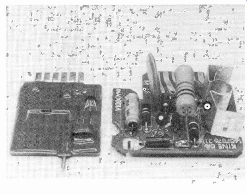
Fig. 12-21. Interior of MAD module from its beginning as a discrete, to thick
film on ceramic substrate, final encapsulation. (Courtesy Gene Lempke)
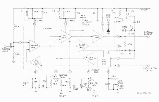
Fig. 12-22. Block diagram of the CA3066 chroma signal processor. (Courtesy
Dick SantiFli)
The CA3067 chroma demodulator and tint control is another 16-pin IC, this time centered on the MAE chroma II plug-in module (Figs. 12-24 and 12-25). Subcarrier reference input is fed from terminal 3 to the tint amplifier. The tint amplifier gain is adjusted by the 25K DC control connected to terminal 2. Q7 base is at AC ground through a 0.01-mfd capacitor at terminal 16. Q2-Q3 is a differential amplifier, with Q3 base-fed from the terminal 3 input. The output of these two amplifiers is mixed in the collector of Q4, and the gain of Q4 and Q3 is adjusted by the tint control for an oscillator mix that results in a certain phase shift for desirable flesh tones. Q8, meanwhile, supplies DC bias for Q4 from the divider network of R2, R5, etc., that extends to the bases of Q6, Q5, and Q1 from the main 11.2-volt supply. Voltage from the Q4 collector passes to the base, then emitter, of Q38 and into the base of differential amplifier Q39-Q7 and out to the RLC phase shift ...
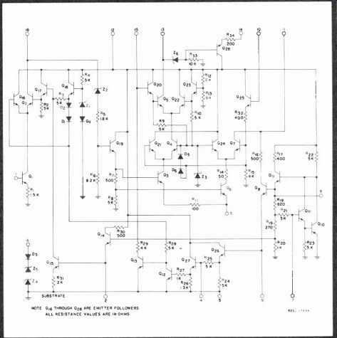
Fig. 12-23. Schematic diagram of the CA3066 chroma processor, IC1.
... network for the amplifier-demodulator input terminals 6 and 12. These passive components determine the phase angles of the sine waves going into the amplifier-demodulators. Terminals 7 and 11 connect to additional emitter bypass filters.
Terminals 6 and 12 may be a little difficult to find, but they are located in the base inputs of Q9 (lowest amplifier) and Q11 (top amplifier), respectively. These two amplifiers are identical and seem to be self-adjusting, since the greater the input the more voltage dropped across R13, for instance. The greater the drop across R13, the less the base input to Q45, and the less signal appears through the emitter of Q44. The same is true for the Q9-Q40 group at the bottom of the schematic. The Q10-Q42 assembly is virtually a regulator for the base bias voltages of Q12, Q19, Q26, Q27, Q34, Q31, and Q28 so that when the main supply changes, Q43 feeds back to Q10, and the DC outputs at the emitter of Q42 is automatically limited or boosted, depending on the drop across R19.
Chroma is applied to the lower Q13-Q14 and Q20-Q21 pairs of differential amplifiers, but only through terminal 14, since terminal 15 is at AC ground and the resonant frequency of the 620-microhenry coil and 0.01-mfd capacitor in series amounts to 63.7 kHz, with the reactance of the capacitor amounting to 1 ohm at 3 MHz. To describe the switching action of the synchronous demodulators: when Q13 and Q20 are receiving chroma, R18 and R28 develop sampling signals that key Q22-Q24 and Q15-Q17. And when R14 and R24 develop subcarrier references and turn on Q23-Q25 and Q16-Q18, synchronous switching develops that produces the R-Y and B-Y outputs from the top and bottom output demodulators which go to Q51 and Q47. The G-Y information is resistively matrixed by R37 and R40 for the Q31-Q33 output amplifier with a Darlington Q48-Q49 driver at its input. Capacitors C2, C3 and C4 are the 7.2-MHz filters that absorb switching transients. Since there is signal inversion in Q9 and Q11, signals to the bases of each pair of synchronous switches are 180 degrees out of phase with those opposite, so one pair switches while the other pair is off.
It's interesting to note that in the Q29-Q30, Q32-Q33 and Q35-Q36 output amplifiers, a bias is developed for Q29, Q32, Q35 in the collectors of Q30, Q33 and Q36. The bias keeps the lower transistors turned on and helps deliver a pair of rein forced, low-impedance, in-phase inputs to the MAD kine driver modules. These MAD modules are a trio of two transistor amplifiers that mix chroma and luminance for RGB cathode drives of the picture tube.
The Accu-Matic in this receiver does about what most other fixed bias systems of this type do: it reduces the blue output, changes the phase angle slightly towards open, adding some red, and enlarges the demodulation angle so that the area of fleshtones is increased.
A ONE-CHIP COMPLETE MONOLITHIC CHROMA PROCESSOR
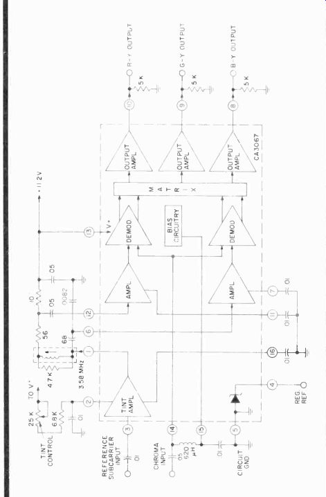
Fig. 12-24. RCA's CTC46, 54 Series CA3067 chroma demodulator functional drawing.
Fig. 12-25. Schematic of the CA3DoY chroma demodulator.
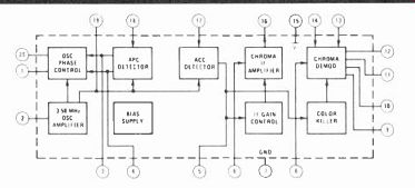
Fig. 12-26
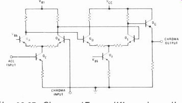
Fig. 12-27
At the June, 1971, IEEE Broadcast & Television Receiver group meeting in Chicago, R & D products showed a complete one-chip color processor. The finished product has a power dissipation of 400 mw, an output resistance of 50 ohms, five alignment adjustments, and 42 external components as op posed to the announced competition which has 62 and 77, respectively, for active 2- and 3-chip circuits. The system is identified as a uA782 chroma processor. A block diagram is shown in Fig. 12-26, while Fig. 12-31 outlines the entire function in what is described by Normal Doyle as a typical application.
The external transistor is a blanker for 3.58-MHz reference signals to the demodulators. Other peripheral components include APC and ACC potentiometers, capacitance couplers and filters, the 3.578545-MHz crystal control for the color oscillator, video input and chroma reference input trans formers. The block diagram (Fig. 12-26) starts with the 3.58-MHz oscillator that supplies the demodulators through pin 19, and the oscillator phase control, ACC and APC detectors, along with an active bias supply. The ACC detector output goes to the IF gain control and color killer, and these two stages act on the chroma IF amplifier and the chroma demodulators, respectively.
Color IF Amplifier (Fig. 12-27)
The basic chroma amplifier comprises two cross-coupled pairs, Qa-Qb, and Qd-Qe, with incoming video applied to the base of Qb from the video detector and the bandpass trans former at an amplitude of from 10 to 200 millivolts p-p.
Automatic chroma control voltage at the base of Qc controls the DC gain of both transistors, with outputs to the bases of Qd and Qe, another differential amplifier supplied by constant current source Qf. Emitter follower Qg is the output with AC at about 2 volts p-p, and this voltage goes into the demodulators through an output that contains both level and tint controls.
Subcarrier Regenerator and Control Circuits (Fig. 12-28)
Again, a current supplying transistor Qc activates the emitters of Qa and Qb, which supplies the 3.58-MHz crystal, its tuning capacitor, and the base of Qd. Qd and Qa form a voltage-controlled oscillator. The oscillator frequency is determined by the voltage difference between the bases of Qa and Qb, which results in drops across R1 and R2 in the collectors of Qa and Qb, and the charging 56-pf capacitor between them.
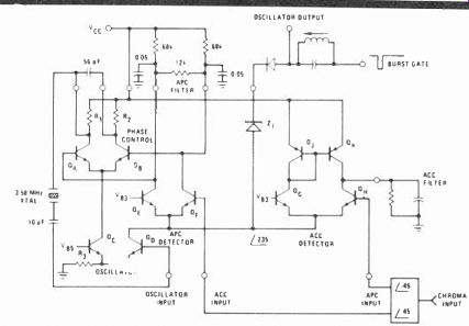
Fig. 12-28. 3.58-MHz subcarrier oscillator, phase control, APC detector,
and ACC detector circuits.
Upon horizontal scan, the collector of Qd rises toward Vcc, back-biasing the emitters of Qe, Qf, Qg and Qh, and allows oscillator current to flow into the external LC circuit, sup plying a pair of reference signals for the demodulators. But when burst appears, the slightly delayed negative horizontal cutoff pulse back biases the "diode," and the oscillator current channels into automatic phase control detectors Qe and Qf and automatic chroma control detectors Qg and Qh. Since plus or minus 45-degree difference phases of burst from the chroma input appear at the bases of Qf and Qh, Qf is turned on and its output goes to Qb and the APC filter to supply any correction voltage needed by the color oscillator. Since the ACC detector is turned on simultaneously with the APC detector, base-coupled Qk and Qj form a balanced-to-unbalanced converter, with initial collector currents equal. The output goes into an ACC filter for proportional DC control of the IF amplifier and color killer circuits.
Fig. 12-29. One half of the chroma demodulator circuit.
Chroma Demodulator (Fig. 12-29)
This type of circuit is simply a lower chroma input stage supplying a pair of 3.58-MHz gated switches that produce R-Y and B-Y chroma demodulated signals, with the G-Y matrixed from the negative outputs of each. A simplified schematic of one-half of the synchronous demodulator is shown in Fig. 12 29, with one reference sine-wave gating input and one chroma receiving terminal. Each composite stage is completely balanced to remove switching voltages, and the three (RGB) Y outputs go into emitter follower drivers for the luminance mix either in additional cathode ray tube drivers or the CRT itself. Phase angles for the 3.58-MHz inputs are tunable so that any CRT phosphor combination or "cosmetic" need may be fulfilled. With the new phosphors, phase angles from about 100 to about 105 degrees are common among the more sophisticated receivers. There are still, however, some X and Z demodulation sets that have phase angles of less than 90 degrees.
Color Killer (Fig. 12-30)
The color killer is a 6-transistor configuration, with a novel input and two pairs of difference amplifiers. But instead of operating on the chroma IF amplifier as is the usual case, the killer removes all signal from the demodulator, thus stopping all color processing.
Transistors Qa and Qb constitute a Schmitt trigger, with Qa normally off and Qb normally on. When the incoming automatic chroma control voltage increases enough to turn Qa on, current is robbed from the collector of Qa, and starved Qb shuts off. Voltage rises to almost Vcc across R2, and turns on Qc hard. The low output at Qa's collector shuts off Qd, Qf then turns on, but Qe is turned off. The DC level to the demodulator continues, but there is no chroma output because emitter follower Qe is not operating. This, Norman Doyle explains, is the reason that the "killer action does not alter the DC level at the demodulator output, thus permitting direct coupling to the video output stages." Fig. 12-31 shows the IC with all peripheral components and connections.
Fig. 12-30. Color killer circuit.
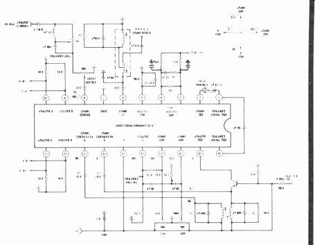
Fig. 12-31. Complete circuit block diagram with all external connections.
QUESTIONS
1. What three inputs must all chroma subsystems have?
2. Where does luminance appear in the chroma circuits?
3. What function does a diode comparator perform for the subcarrier oscillator and first bandpass amplifier?
4. Is the fixed phase angle of the demodulators shifted internally or externally prior to demodulation?
5. In any graphic display of reactance, a capacitive Xc is always shown in what direction?
6. Name the three phase angles normally used in color demodulation? How are they decided upon?
7. In the early receivers, where were chroma and luminance normally matrixed?
8. How are the green colors normally derived by most demodulating systems even today?
9. What is the advantage of color CRT cathode drive?
10. Name the frequency to which all other sync frequencies in the color transmission system are slaved? 11. How much phase shift is there between I and Q and R-Y, B-Y?
12. The chroma input is limited to a 1-MHz bandpass between what two limits? What two sidebands? 13. If you have chroma cutoff only, what control would you automatically adjust first to see if it was at fault?
14. Why must color amplifiers or luminance-chroma amplifiers be cut off during retrace times?
15. How can you tell the least and most efficient phosphors of a CRT with a rainbow pattern RF input?
16. Does the Motorola MC1398 color processor have a phase comparison correction for the 3.58-MHz oscillator or an injection lock?
17. What is unusual about the MC1398's color killer?
18. In how many phases are the 3.58-MHz signals applied to the IC demodulator?
19. What does Motorola's Instamatic feature accomplish in the chroma circuits?
20. What's another trade name for Instamatic?
21. What does Instamatic control?
22. Synchronous detection can also be called synchronous s g.
23. To align Zenith's three-IC chroma subsystem, how many transformer adjustments are there?
24. Chroma alignment, including crosstalk adjustment, requires the use of what two instruments?
25. Does the color killer in the Fairchild-Zenith IC group affect both sets of chroma amplifiers?
26. Are modern CRT phosphors the same as those originally specified by the NTSC?
27. Does the uA780 have an injection lock on solid-state comparator subcarrier oscillator correction? 28. In a crystal ringing circuit, what must be observed?
29. What is a prime advantage of a crystal ringing circuit?
30. In the CA3067 chroma demodulator, complete the statement, "each pair of synchronous switches are 180 degrees .
31. What special circuit characterizes single chroma processor chips put together by Fairchild and Warwick?
32. What color cutoff circuit is common to both the Motorola and Fairchild chroma processor chips?
Next: Link | --Transmission Lines & Antenna Systems
Also see:
TV Antennas and Transmission lines
Air Time--An Intro to Television Broadcasting
TV and Radio Tube Troubles (1958)