Video detectors and video (luminance) amplifiers are being given considerably more attention as chroma processing and picture tubes improve so that maximum video detail and resolution can be supplied to the overall system. Our initial block diagram (Fig. 6-1) is much like the one in Section 1.
DC SIGNAL COMPONENT
Norman Doyle and Don Smith of Fairchild Semiconductor say: "the DC component of a television signal contains in formation relating to the mean brightness of the scene being televised." So if there is no DC component, mean brightness is AC coupled and only picture content determines the average value of video voltage-and this isn't good. Therefore, you must either DC couple all video amplifiers to the picture tube following the video detector, or find some means of restoring the DC level.
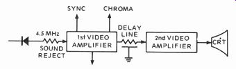
Fig. 6-1. Conventional video detector and video amplifier block diagram.
In color receivers, there are three color difference voltages to contend with, and AC coupling could only produce a background tint proportional to the mean values of all three signals. In DC restoration or coupling, you fix a DC level and then position black and white levels with respect to it. And you must be sure, according to Doyle and Smith, that the contrast gain control and various signal conditions do not upset this fixed DC level. Also, an all-DC-coupled system will cause the ...
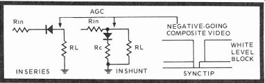
Fig. 6-2. Half-wave video detector diode in series and shunt, depending on
bias, source and output impedances. Both pass only negative-going demodulated
video as shown.
... receiver cathode ray tube to go white to the point of blooming with no incoming signal because of negative carrier modulation, and the absence of carrier means "whiter than white." Black level clamping, therefore, is normally used in most systems, along with some slight capacitor coupling, at least in the luminance channels. With no incoming signal, then, the CRT is dark and excessive current isn't drawn.
To translate, getting undistorted television signals to the chroma and luminance amplifiers has always been a problem because of the characteristics of the video detector diode. And although the old faithful germanium diode in most systems works fairly well, it is basically nonlinear. Any uses unidirectional characteristics of doping and crystalline structure to produce an output voltage proportional to the level of detected modulation-less a 0.2-volt drop. The operation equation may be set forth in terms of current:
i = {g/(1+9R1)} ei
where g is diode conductivity, R1 the terminating impedance, and ei, the input voltage. Diodes may be connected in series or shunt, depending on biasing and the source and load impedances (Fig. 6-2). Both diodes, in these examples pass only the negative half on the demodulated waveform. If an effective 2-diode arrangement, such as outlined in Fig. 6-3, were designed, there would be considerably less harmonic distortion because of full-wave rectification, and the carrier frequency would be doubled, cutting most distortion in half.
DIODE DETECTORS AND VACUUM TUBE VIDEO AMPLIFIERS
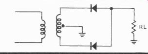
Fig. 6-3. Full-wave video detector diode circuit, which is not practical
for color TV in the simple form.
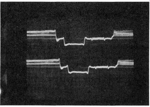
Fig. 6-5. If you want to check a delay line and see if it's actually working,
here's how. The scope's time base is set at 2 microseconds per division. The
delay is 0.8 microsecond; count it!
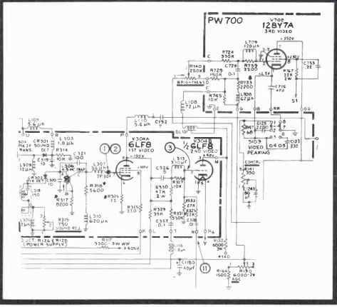
Fig. 6-4. Vacuum tube video amplifiers in the RCA CTC25 series.
In tube receivers, only half wave diode detectors have been used for sound and video detectors as illustrated in Fig. 6-4. Here, both diodes pick off positive or negative modulation for the respective circuits, and video passes over the 4.5-MHz carrier sound trap as described in Section 5. First video amplifier V304A is de-generatively biased with a 22-ohm cathode resistor. There is a series peaking coil in the plate circuit, along with additional peaking and LC resonant circuits in the coupling and grid circuits of the second and third video amplifiers. The plate and screen grids of the first video amplifier supply signals to the AGC and sync circuits, plus chroma signals to the bandpass amplifier grid (not shown).
The second video amplifier grid circuit is rather heavily endowed with both noise cutoff and vertical interval blanking inputs, plus sync-stripped video from the first video amplifier.
V304B passes the luminance signal through 0.8-microsecond delay line DL101 (Fig. 6-5), and into the grid of the AC-coupled third video amplifier, the driver for the CRT cathodes. Notice in the photograph that the trailing edge of the lower trace is delayed exactly the 0.8-microsecond interval, since the oscilloscope's time base was set for 2 microseconds per div.
Squiggles (9 of them) following the horizontal sync pedestal are the 9 cycles of color sync burst. The scope's vertical amplifiers were set to alternating since this frequency is much too fast for a chopped input. Actually, we put the scope on 10 microseconds per division and used a X5 extender (now 2 microseconds per division) to precisely show these two signals across the delay line. Another very useful application for a good oscilloscope-and the only simple way to discover if a delay line is good or not.
High-frequency compensation is normally provided by shunt peaking with a coil, but series coil peaking isolates the effects of input and output capacitances, and so offers an advantage. Combined, shunt and series peaking permits higher gain than either used singly. Low-frequency compensation is usually added with an RC combination filter somewhere in the plate circuit of the video amplifier. Also, the value of the cathode (or emitter) bypass capacitor largely determines the low-frequency response of an amplifier.
BRIGHTNESS LIMITERS, BLANKERS & VIDEO AMPLIFIERS
In Zenith's C4030 video circuits (Fig. 6-6) composite video is coupled into second video Q205 principally through capacitors C213, C214, and partially through the contrast control. DC is applied through contrast R230 from the 24-volt line as forward bias, shown as 3.25 volts on the base of the transistor. Q205 has a 1.3K load resistor connected to the 24-volt supply line on one side of the collector, and series peaking coils L202, L204, and the L203 0.8-microsecond delay line in between. Signals out of Q205 go directly to the base of the Q206, the third video amplifier. The normal-setup switch in the emitter circuit removes video in the setup position.
Out of the emitter of Q205 is an RLC network that includes the brightness control and vertical blanker. The base circuit of Q205 contains the brightness limiter. This latter circuit senses excessive beam current by monitoring the current out the high-voltage tripler. The brightness limiter input is clamped by Zener CR214 and thus is protected against excessive high-voltage arcs. If the HV current flow rises above normal, Q204 acts as a partial or complete switch and drops the voltage from the 24-volt supply across 10K R228 so that the contrast control and, therefore, the base of Q205 receives less positive voltage or forward bias. The lower bias reduces the conduction of the second video amplifier and its signal current output and so controls the CRT beam current.
The vertical blanking circuit receives a positive pulse from a winding on the vertical output transformer. Emitter-follower Q207 applies the pulse to the emitter of second video amplifier Q205. At the end of each 15.2-millisecond vertical trace interval, the vertical output transformer furnishes an inductive kick of 23 volts p-p, turns on the Q207 vertical blanker, and the 18-volt pulse as its emitter firmly back-biases the emitter of the second video amplifier, thus cutting off the transistor. Across the 470-ohm resistor, also at the emitter, an 11.1-microsecond horizontal blanking pulse arrives following the 52.4-microsecond forward line scan. This pulse also turns off Q205 by back biasing.
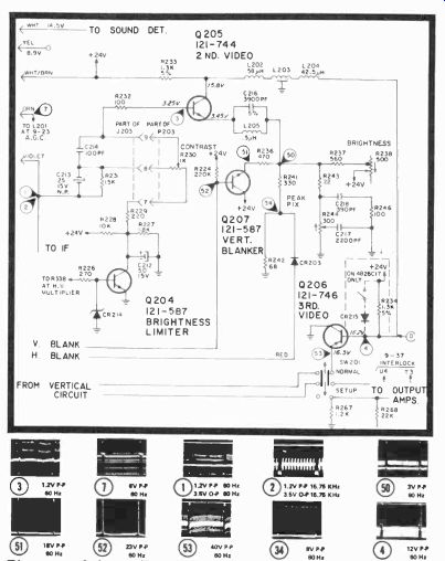
Fig. 6-6. Schematic of Zenith's 4 B25C19 Series video amplifiers, as well
as brightness limiter and unique vertical and horizontal blanking circuits.
Very simply, both horizontal and vertical blanking are achieved in a single stage with a minimum effect on the second video amplifier, since there is no overstressing caused by the simple cutoff bias. Video circuits must always be blanked at the horizontal interval, you may recall, because that is the time the horizontal sync pulse is transmitted as well as the 3.58-MHz color sync burst. The vertical interval of 1.4 milliseconds per field is used for reception of vertical, horizontal, and equalizing pulses.
Notice, also, the voltage dividers among the various transistors, the direct (DC) coupling, and the relatively few peaking and choke coils that are designed into the circuits. In dealing with transistorized receivers, you will find this is a normal condition rather than an unusual one. Once you understand transistor operation and have a good grasp of biasing and gain, such circuits should be considerably easier to troubleshoot. In our investigations, we have always found that in solid-state work a DC amplifier, triggered oscilloscope is indispensable. Sincerely, we doubt if you can get along without it. For instance, do you really have a meter that will measure 3.25 and 3.45 volts at the base-emitter of Q205? And if you can measure the voltage with a meter, is Q205 being blanked during the horizontal and vertical intervals at the proper times, and is its video output adequate? Worthwhile questions for, we hope, receptive minds.
As we have stated, germanium diodes used as video detectors have served useful purposes throughout the years, but are fundamentally nonlinear. And when current gain in any third or fourth-stage video IF amplifier reaches a certain point and begins to decline, the amplified output will be somewhat nonlinear. This is illustrated in Fig. 6-7 and is taken from Application Note AN-545, authored by Terry Kiteley, Motorola, Phoenix. Additionally, forward impedance characteristics of the detector diode's germanium material add to this nonlinearity.
These dual nonlinearities produce sum and difference beats called "tweets," which can always combine with the video signal or radiate back into the IFs and even to the receiving antenna, causing sync and video instability as well as external interference. TV manufacturers, Kiteley says, use various types of filters and shields to minimize these effects.
But he also points out that a good low-level detection system without the traditional germanium diode would do away with these problems more easily.
In Fig. 6-7, the modulated video carrier is outlined and shaded at the bottom, while the output is strongly influenced by the curving dark line between diode and transistor hfe, and is shown both as white level compression and sync pulse distortion.
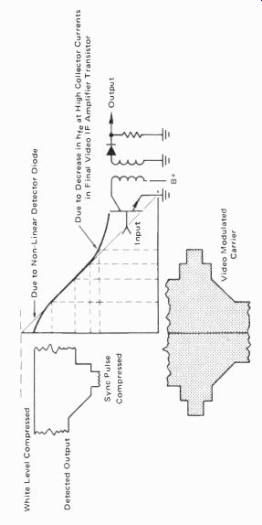
Fig. 6-7. Last video IF and diode detector transfer characteristics showing
the usual nonlinearities.
In place of the diode, Kiteley proposes a doubly balanced, full-wave, synchronous detector (you'll see more of this when we're discussing chroma demodulators) wrapped up in a convenient 8-pin plastic in-line package with a conversion gain of 34 db, a video frequency response of 6 MHz, and video output of 7.7 volts p-p. The linear transfer characteristics are exhibited in Fig. 6-8. The line between transistor output and diode output is straight, with an undistorted output and neither sync nor video compression. A schematic of the unit, including IF input and video output, is illustrated in Fig. 6-9, while a block diagram for such a detector is exhibited in Fig. 6-10. The video modulation is amplified and limited, passed to a full-wave multiplier for delivery to a low-pass filter and the video output.
In the simplified schematic in Fig. 6-11, transistor Q7 is a forward biased constant-current source. Q1 and Q2 form a differential amplifier, with the base of Q2 at AC ground and the modulated carrier applied to Q1. Pairs Q3, Q5 and Q4, Q6 are the in-out phase clipped carrier-operated synchronous switches. Waveforms on the right side of the illustration show the Q1, Q3, and Q4 base inputs, and the resulting full-wave output developed across R1.
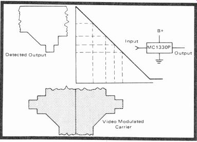
Fig. 6-8. MC1330P linear transfer characteristics. Notice there is no sync
or video compression.
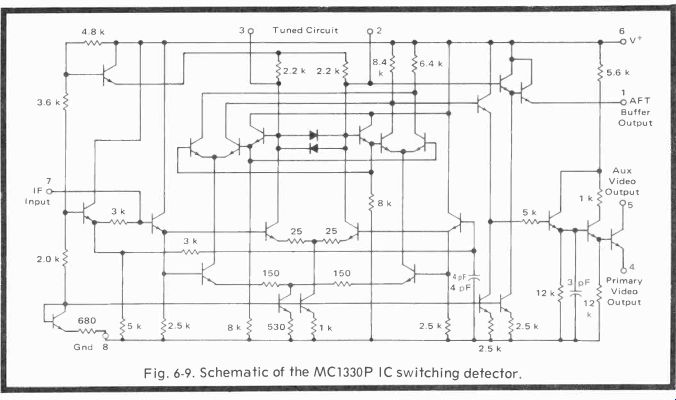
Fig. 6-9. Schematic of the MC1330P IC switching detector.
If an in-phase clipped carrier (Fig. 6-11B) is applied to Q3 and Q6, and the negative-going modulated carrier goes to the base of Q1, any possible Q1 conduction would back bias the Q3-Q5 pair of switches because of phase inversion, but turn on Q2 without phase inversion and Q6 would conduct. Current would, therefore, flow through R2 and produce an output. If Q1 were fully back biased, Q2 would conduct through differential action and turn on Q6 anyway. When the modulated carrier has larger positive incoming signals, Q6 is nonconducting because Q2 is off, while a negative voltage forward biases Q3 and produces an output across R1. With a change in clipped carrier phase, Q4 is turned on by Q2's conduction. Then, with a modulated carrier phase reversal, Q5 operates, since Q1 conducts negatively and forward biases its emitter, increasing the current across R2.
This is called synchronous detection. First one and then the other switches operate as clipped carriers while modulated carriers go through a phase reversal and develop currents across R1 and R2. This action, of course, causes the detector to be switched at twice the carrier rate, leaving no original carrier present, but simply modulated pulses that are double those of the original carrier frequency (Fig. 6-11D).
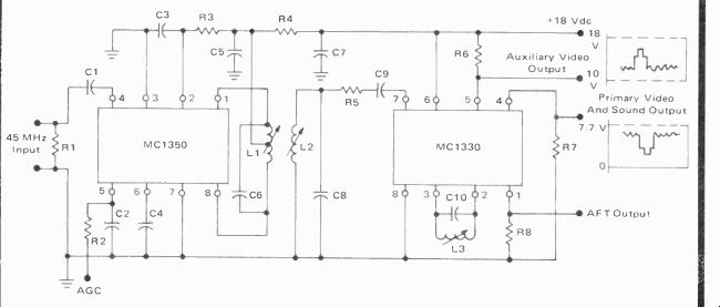
It is important that switching voltages contain only carrier energy and not color information. Therefore, this external circuit must have a filter such as L3 and C10 in Fig. 6 12. The figure shows two integrated circuits, the first two video amplifiers (MC1350), including AGC amplifiers and bias supplies. The second MC1330 device (schematic in Fig. 6-9) is the circuit we've been looking at, which also contains the third video IF. As you can see in Fig. 6-12, there are still coils to be tuned (the T1 coupling transformer between integrated circuits), so we don't have a transformerless video IF yet. At the outputs of MC1330 are two out-of-phase video signals, either of which may be used. The two signals are simply the emitter and collector outputs of the output transistor shown in Fig. 6-9.
FM DETECTION & AUDIO AMPLIFIERS
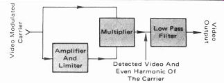
Fig. 6-10. Block diagram of the MC1330P.
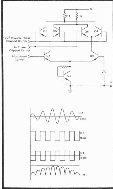
Fig. 6-11. Simplified schematic of the MC1330P and switching waveforms.
Fig, 6-12, IF system using an MC13SO (two F amplifiers) and an MC1330 (final
F and synchrotious detector).
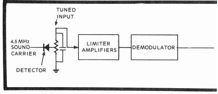
Fig. 6-13. Block diagram of a typical audio system showing detector diode,
amplifiers, demodulator, and two stages of audio amplification. The speaker
in more recent receivers may be capacitor or transformer coupled.
TV receiver audio systems have been taken pretty much for granted these last 20 years because there really wasn't much to them except rather inferior sound delivery. It all began with the good Foster-Seely discriminator that was somewhat susceptible to noise. Sound systems evolved to the popular ratio detector which was more noise immune, then came the pentode quadrature gated-beam detector and the locked-grid detector. Today, an ever increasing number of integrated circuit amplifiers and detectors are appearing, and at least one all-ceramic throw-away output stage is in use.
TV audio systems are limited to a 50-kHz bandpass, rather than the 150-kHz bandpass reserved for FM and FM stereo. So you can't expect overwhelming fidelity nor sound-surrounding output. Nonetheless, with the advent of ICs and better designed push-pull output stages that no longer use trans formers, the quality of TV sound has improved remarkably.
This is due to the self-limiting characteristics of the internal amplifiers, more precise demodulation, better de-emphasis and tone networks, more powerful and efficient outputs with less built-in distortion, and good impedance matches with an output coupling capacitor in place of the usual lossy trans former. The large bandpass of more recent power transistors has aided, too.
A block diagram of a conventional TV sound system is shown in Fig. 6-13. Sound is picked off at the video detector by a sound detector diode, put through a 4.5-MHz FM audio carrier tuned circuit and fed into one or more limiting amplifiers. After FM is demodulated and de-emphasized to counter transmitter pre-emphasis, the audio is amplified in two stages and coupled to the speaker. The "cheapies" chop this sound procedure down somewhat, but all such subsystems are basically the same. The big difference exists in FM-to-audio detectors, and the less expensive receivers almost inevitably use a type of gated-beam detector, since demodulation requires a single tube or perhaps one or two transistors.
Otherwise, the block shown is just about what you should expect to find in any receiver on the market.
Discriminator This forerunner of FM detectors dates back to much earlier days when frequency-modulated radio was a novelty, so obviously it isn't especially recent or unique. But the sound it produced was good, and some radios today may still be using the idea, if not the circuit.
Referring to Fig. 6-14, both primary and secondary circuits are LC tuned to the 4.5-MHz incoming carrier, and the signal is electromagnetically and capacitively coupled from primary to secondary. If the signal is exactly on frequency (carrier frequency), each of the secondary diodes receives 90 degree out-of-phase signals, and the rectified output currents develop equal and opposite (canceling) voltages across R2 and R3. When the frequency of the input signal varies below or above 4.5 MHz, the diodes-180 degrees out of phase with one another-develop relatively positive or negative outputs that reflect the degree of higher or lower incoming frequencies (modulation). The changing carrier frequency generates audio voltages that are proportional in amplitude to the FM broadcast deviations. You can always recognize an F-S discriminator circuit by the two detector diodes in parallel and the small capacitors.
Ratio Detector
The unbalanced ratio detector (Fig. 6-15) looks much like the F-S discriminator, except it has series instead of parallel ...
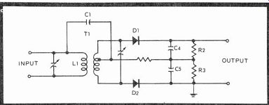
Fig. 6-14. Durable Foster-Seely discriminator circuit.
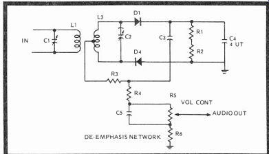
Fig. 6-15. An F-S successor, the unbalanced ratio detector which is less
susceptible to AM noise.
... diodes, and includes a big capacitor across load resistors R1 and R2 to ground. Because of C4, the circuit's load voltage cannot follow small changes in the input signal and is, therefore, not sensitive to incoming amplitude variations.
Phase differences between secondary and primary, and on either side of the tapped transformer secondary, are the same as in the F-S discriminator. However, since the detector diodes are in series, they generate a constant sum total of output load voltages at all times, but their ratio varies with the input signal deviation. The output is a changing ratio across the output resistors rather than a pure voltage difference. This is why such a circuit is called a ratio detector. Since the circuit always has a DC output, coupling capacitor C3 is installed to supply an AC-only audio voltage to the de-emphasis network and the audio gain potentiometer.
In both the F-S discriminator and the ratio detector, as the input frequency passes above or below the resonant frequency, current in the transformer secondary lags or leads the induced voltage. And since voltages across the secondary coils lag the secondary current by 90 degrees, the voltages across these coils are then 90 degrees out of phase with the primary voltage when the received frequency matches the tuned resonant secondary.
Vacuum Tube Sound
Subsystems RCA's CTC25X chassis sound system is most representative of the middle '60s era (Fig. 6-16). Sound is picked off by a positive demodulating detector diode in the plate circuit of the third IF and brought to the grid of the sound IF (V201) through an RLC network following the diode and another blocking capacitor, plus additional series and shunt coils that reject video and sync and form a tuned 4.5-MHz circuit.
The 6EW6 tube is a sharp cutoff pentode used in gain controlled audio and video IF stages. It features controlled plate-current cutoff and a high transconductance of 1400 micromhos. It's relatively large plate swing, along with the other characteristics, provides considerable gain so that only one stage is needed before demodulation. The sound IF (T202) transformer is double tuned for broad bandwidth, with a resonant circuit in its secondary, which is a good impedance match for the grid of the following sound demodulator.
The 6HZ6 demodulator is a sharp cutoff pentode with two independent control grids. It may be used either as a Class A amplifier or as an FM sound detector in FM and television receivers in either parallel or series-connected heater strings.
Used by both Zenith and RCA in much the same configuration, the circuit is similar in many respects to the old 6BN6 gated-beam detector, which had a rectangular cathode surrounded on three of its four sides by a focusing anode. Electrons leaving the cathode form a sheet-beam for the focusing anode, go through a narrow slot in the accelerator to the first control grid. If the control grid is slightly negative or positive, electrons may pass, but otherwise they are blocked and return to the cathode. The control grid, meanwhile, is saturated by large positive signals or cut off during negative signals and so limits the received FM signal amplitude. When the control grid allows electrons to pass, they go to a second accelerator, the screen grid, and on to the quadrature grid, connected to a 4.5-MHz high Q resonant circuit consisting of the RLC network between ground and pin 7.
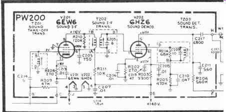
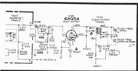
Fig. 6-16. RCA CTC25X vacuum tube sound subsystem circuits.
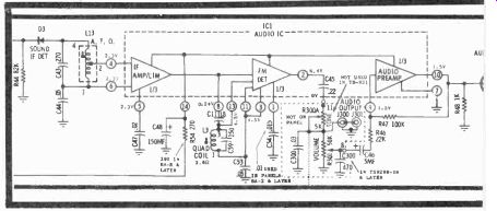
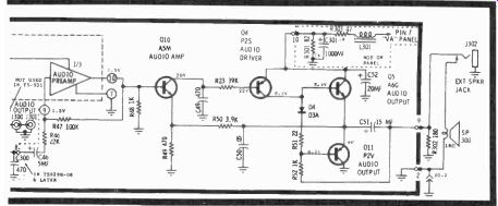
Fig. 6-17. Schematic of Motorola's CTV7-8 audio circuits.
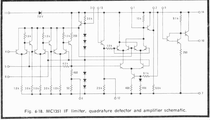
Fig. 6-18. MC1351 IF limiter, quadrature detector and amplifier schematic.
When the incoming signal is exactly 4.5 MHz, the tuned quadrature grid lags this frequency by 90 degrees. Higher frequencies cause larger phase lags and lower frequencies lesser lags. The combined effect of the two grids cause different pulse current widths to arrive at the detector plate, making the plate current a linear function of FM deviation.
Audio voltage is developed across load resistor R206 and passed through a de-emphasis RC network and the volume control to the grid of the audio output. Notice that the tone control is in parallel with half of the volume control and is simply an RC series pair of components that can attenuate the higher frequencies, with possibly a boost for the low ones.
The 6AQ5 audio output cathode is heavily bypassed, thereby allowing the tube to work virtually at full potential and deliver several watts of output. The suppressor grid is at cathode potential, while the screen is supplied by the +140-volt source. Capacitor C139, between plate and screen, is a basic troublemaker if its transient suppression and stabilizing function is disturbed, especially by a short. The primary of output transformer T103 often opens because of the 405-volt supply and high current demands of the output tube.
Motorola's CTV7-8 audio subsystem Fig. 6-17) uses an IC and a push-pull capacitor-coupled output. However, the solid state FM detector does have a quadrature coil like the 6HZ6 tube, and so also is known as a quadrature detector.
The FM sound takeoff point is in the collector of the third video IF transistor. The 4.5-MHz signal passes through the sound IF detector into the (L13, C43, 44) 4.5-MHz tuned input circuit. The IC input is terminal 4, since terminal 6 is actually a bypassed bias supply.
The IC itself is also quite interesting and is a Motorola type MC1351. It is a dual in-line monolithic IC with 22 transistors, 7 diodes, a zener diode, and 21 diffused resistors. It has three limiting differential amplifiers (Fig. 6-18), voltage regulation by the 7-volt zener and diodes D1-D6 plus Q10, an effective means of quadrature demodulation, current-multiplying drivers and an emitter-follower final stage serving as a low-impedance preamplifier.
The three differential amplifiers, each with a gain of 10, are buffered by emitter-follower outputs. The amplifiers are limited in output swing for excellent AM rejection and furnish a total 60 db gain over the frequency range of 1 to 12 MHz.
Following the six temperature-compensating and regulating diodes are another two pairs of cross-coupled differential amplifiers supplied by a single transistor current source and another feeder pair, again differential in configuration. The right-hand transistor of this pair has a regulated DC voltage on its base, while the basic FM signal is delivered to the base of its sister transistor on the left from the third buffer transistor following the three limiters.
On the schematic (Fig 6-17), a quadrature coil and shunting 150-pf capacitor form a tank circuit, the Q of which determines the peak separation of the detected output, noise characteristics, and output voltage swing of the detector.
Since this is a quadrature system, the tuned circuit will lag the incoming carrier by precisely 90 degrees. The output, through the emitter follower transistor to pin 2, is twice the input through pin 13, the initial emitter-follower and the 1K limiting resistor. The time constant of the 10K resistor in the right differential amplifier and the 0.015-mfd capacitor (normally the de-emphasis network) shunts the twice multiplied incoming frequency and any noise pulses to ground. Higher frequencies result in a greater phase lag and lower frequencies produce a smaller phase lag, with maximum output at 0 degrees and-or 180 degrees.
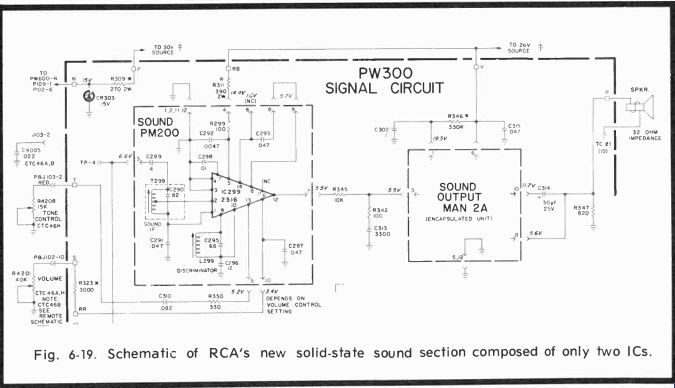
Fig. 6-19. Schematic of RCA's new solid-state sound section composed of only
two ICs.
These differential amplifiers are, in reality, switching circuits that combine the varied pulse transitions through the emitter follower transistor (pin 2) and develop an audio output that is a linear function of frequency deviation. The recovered sound is then passed through pin 9 into the audio preamplifier current driver transistors and out through the emitter follower at pin 10, with some stabilizing feedback returning to pin 9.
Further amplification is provided by Q10 and Q4. Q4 is a class B (approximately) push-pull output coupled through a 150-mfd capacitor directly to the speaker.
In the complementary symmetry output stage, as it's called, the NPN-PNP coupled emitters are quiescently biased at 10.7 volts. The upper NPN base has 11.2 volts and the lower PNP base has 10.2 volts. Since the NPN's base-to-emitter voltage difference is +0.5 volt, and the PNP's base-to-emitter voltage difference is-0.5 volt, both transistors are forward biased to within 0.2 volt of conduction, also an antidote for crossover distortion. A positive audio voltage will drive Q5 into conduction, and a negative audio voltage will pass DC for ward-biased D4 and drive Q11 into conduction. The outputs are then coupled through C51 to the speaker. Resistor R50 supplies feedback, to the emitter of Q10 for DC stability and to minimize distortion at high output levels. R51 and R52 are simply the voltage dividing network for the base of Q11, while R302 is part of the load and charging path for C51.
RCA's 2-stage IC thick film audio processor is represented in Figs. 6-19 through 6-22. Since an entire integrated circuit is obviously more expensive than several individual transistors, manufacturers must have reasons for going substantially all-IC. The CTC46 and CTC54, two new RCA solid-state chassis, have supplied many of the answers, except cost, and we'll probably never know this. However, the circuit on board PW300 consists of only three basic entities: one monolithic IC299, one phenolic encapsulated thick film IC, and one speaker. If you count the peripheral components, they amount to about 22 passive pieces-a far cry from almost hundreds used in other sets. So the initial answer here is economy of parts and low labor costs, since the PM200 sound section is a plug-in module, and so is the MAN 2A.
IC299 is a CA3065 complex multifunction IC (Fig. 6-20) with an IF amplifier-limiter supplying an FM detector. The detector output goes to an electronic attenuator, to a buffer, and then to an audio driver and the MAN module. The block diagram, of course, is a "typical" circuit application that makes the routine look easy. But let's go to the schematic (Fig. 6-21) of this little 14-pin IC and you'll get a different perspective.
Incoming sound, applied to terminal 2, passes through the Q11 emitter to the collector of Q12 without inversion, is coupled emitter-to-base to another set of differential amplifiers, Q14-Q15, then delivered to a third set consisting of Q18 and Q19 still in phase. Reference zener D2 and regulators Q1, Q3 and Q4 supply collector regulation for Q12, Q15 and Q19, and detectors Q22 through Q27. The bases of Q17 and Q20, are clamped by D7,...
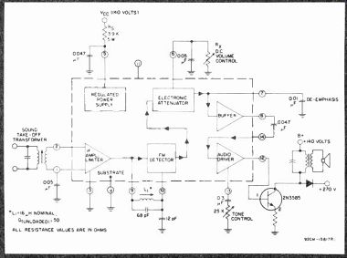
Fig. 6-20. A block diagram of the CA3065 in a typical circuit application.
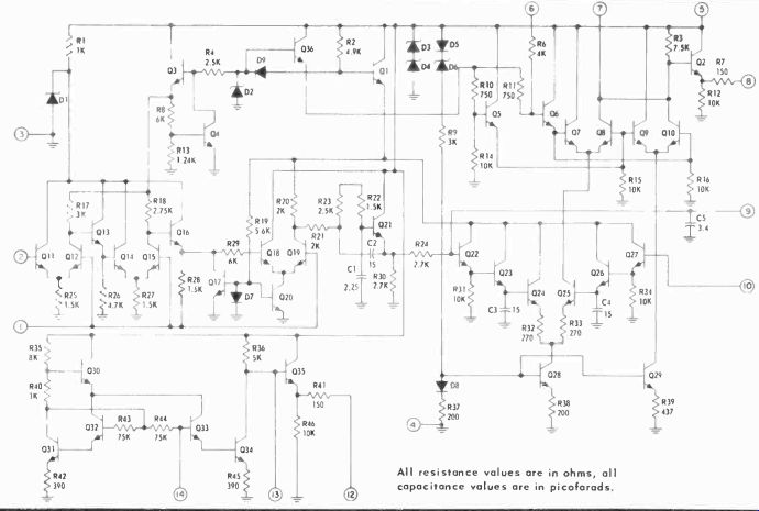
Fig. 6-21. Schematic diagram of the CA3065 IC Sound detector.
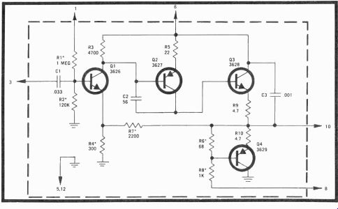
Fig. 6-22. Schematic of the MAN 2 Module phenolic version.
...a limiter and current source, respectively. The Q18-Q19 differential pair again amplifies without phase change through Q21 (with feedback) and to the Q22 and Q27 buffers through the L1-68-pf tunable discriminator circuit (Fig. 6-19) Q23 and Q26 are peak detectors that supply differential amplifiers Q24 and Q25 with detected FM that is compared against the resonance set up by the discriminator circuit so that output currents are proportional to the input FM deviations. After amplification by Q7-Q8, signals are applied to the electronic attenuator.
Terminal 6 is the DC volume control connection, while bias for Q5-Q6 and, subsequently, bias for the bases of Q8-Q9 and Q7-Q10 is supplied from the emitter of Q36 out of the regulated chip supply. Q29 is the emitter constant-current source for Q9-Q10. If you look at these two pairs of differential amplifiers, you will find that, except for the emitters, they are in parallel. The only mobile connection is to the emitter of Q7-Q8 and this is clamped by the limited voltage from the power supply, base bias and the constant current feed from Q29. The output through Q2 and terminal 8, therefore, is electronically and automatically attenuated regardless of incoming signals.
Low-impedance audio is delivered from terminal 8 to terminal 14, the input to buffer Q33 and audio drivers Q34 and Q35. Transistors Q30 through Q32 are simply another regulator, this time for Q33. Any external changes are sensed by the base of Q30 which increases or decreases the emitter current and also the collector current of Q32, which finally reaches the base of Q31 where the change is resistively con trolled by the conduction of this transistor.
The MAN 2A module (Fig. 6-22) receives its input from terminal 12 of PM200 through a 0.033-mfd capacitor between base bias resistors R1 and R2. The signal is amplified through Q2 with a little degenerative feedback to the base of Q3.
Transistors Q3 and Q4 constitute a Class B push-pull amplifier, with Q3 taking incoming voltages from Q2; Q4 requires negative polarity inputs on its base or positive inputs on its emitter. Feedback applied is through terminal 8, following the 50-mfd capacitor at output terminal 10.
QUESTIONS
1. What would the face of the CRT look like in an all DC coupled system with no incoming signal?
2. Why is black level clamping preferred?
3. Are video detector diodes quite linear?
4. Why is there a luminance delay line, and how much is the delay introduced?
5. What is the only way a serviceman has to check a luminance delay line accurately?
6. In the newer receivers, where the vertical and horizontal blanking pulses applied?
7. What happens in the luminance amplifier during vertical and horizontal blanking times?
8. What are "tweets"?
9. How can we be rid of tweets?
10. What's the bandpass of most TV audio sections as opposed to those of FM stereo? 11. What was the first good FM audio detector? 12. Do IC detectors and amplifiers produce better sound than discretes? 13. The ratio detector diodes are connected in p while the discriminator's diodes are in s 9 14. What is the basic difference between the ratio detector and discriminator?
15. What is the fundamental principal of the gated-beam detector?
16. What's different about Motorola's output stage in Fig. 6-17?
17. Can you guess how Q4 in Fig. 6-22 works?
Next: Link | --Sync & AGC Circuits
Also see:
TV Antennas and Transmission lines
Air Time--An Intro to Television Broadcasting
TV and Radio Tube Troubles (1958)