AFC diodes and the associated circuits have been tough cookies in one way or another for a long time, and designers approach new applications with more than a little caution. For instance, in working with AFC diodes, you must be aware of the circuit's hold and pull-in ranges, residual phase differences, noise-bandwidth, pull-in time, and damping factor, plus other lesser known considerations. One of these is the interaction between AFC and AGC systems, especially when the AGC time constant is reduced to allow faster IF bias response. This decreases the horizontal AFC's pull-in range, increases the video IF response and detector output, and so increases ripple voltage output. Sync tracks the ripple only where it increases sync amplitude and, since it will not track in the opposite direction, the sync train to the AFC diodes is incomplete, and this decreases the loop gain of the automatic frequency control system, retarding its efficiency and causing possible horizontal sync-hold problems.
The ripple voltage mentioned is produced during the short-period coincidence of the broadcast sync signal and flyback feedback to the AFC diodes. At that point, the tuner and IF stage gain is reduced, which lowers the video input to the AGC system. As the cycle repeats, a ripple voltage develops that is the frequency difference between the in coming 15.734-kHz horizontal sync pulse and the AGC-RF-IF loop relation.
There are other problems in horizontal circuits such as the design of transistorized horizontal output amplifiers, the switching time, secondary breakdown, power handling, and thermal (temperature) stability. Saturation losses in such transistor amplifiers occur during forward scan periods, and will increase rapidly with higher temperatures. But the largest loss is at fall or turn off time when high voltages and currents coincide, causing the highest collector dissipation. Obviously, heat sinking to take care of this dissipation is more important, and the transistor(s) must have good contact (often silicon grease) to maintain adequate thermal dissipation. Precisely the same considerations apply to silicon controlled rectifiers, such as those used in pairs by RCA for forward trace and retrace drive times. And, we might note, if semiconductor horizontal output stages are driven too fast by a runaway oscillator, they will heat somewhat proportionally to the cyclic rate, quickly turn red, and silently fade away, leaving no high voltage and an interesting repair problem for the service shop.
HORIZONTAL BLOCK DIAGRAM
The horizontal block diagram in Fig. 9-1 is somewhat reminiscent of the vertical circuits, except that feedback and sync comparison circuits are more elaborate, and the entire system operates at about 263 times the vertical rate 59.994 Hz x 263 equals 15,734 Hz, or thereabouts at slide rule accuracies.
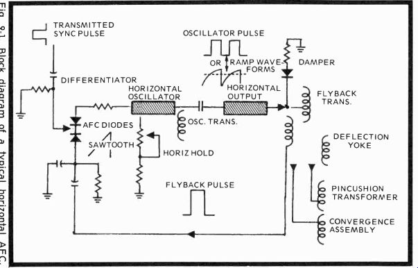
Fig. 9-1.
Differentiated broadcast sync and flyback sawtooth feedback pulses meet at the AFC diodes, which by conducting relatively positively or negatively on resolved phase-and-or frequency differences, deliver a plus or minus DC correction voltage to the horizontal oscillator to keep it on frequency.
Some oscillators have blocking transformers, others are RC coupled, and still a third group features sine-wave output coils that are tunable for the correct sine-wave symmetry. Many horizontal hold circuits are standard variable resistances, except Zenith, for instance, where the hold control is the tunable oscillator coil.
In semiconductor circuits, the oscillator drive and output waveforms are pulses, while in vacuum tube receivers the drive voltage for the output is a ramp-type exponential waveform that turns on the output tube at about 3/4ths of the waveform peak. The output conducts at a horizontal rate, firing the flyback to drive the deflection yoke as well as producing additional voltages for the pincushion transformer and convergence assembly. The damper, if there is one, conducts after the horizontal blanking interval. The collapsing magnetic field during retrace snaps the horizontal sweep back to the left side of the tube and then helps move the trace on its way toward center. Forward scan, of course, propels the trace from the center to the right edge of the CRT, completing the forward sweep.
The damper has a basic function other than helping to move the trace, however, and this is doing what its name implies. The inductance of the horizontal output transformer and the deflection yoke become a resonant circuit with the internal distributed capacitance. When forward trace has...
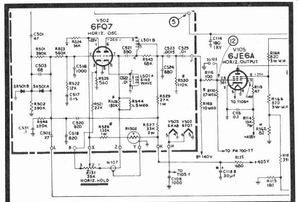
Fig. 9-2. Schematic of an RCA vacuum tube horizontal oscillator-output circuit
used in 1966-1967.
...ceased, an oscillation begins because of shock from magnetic reversal of the system and the generated high voltage. Were this oscillation permitted to continue for any period, there would be a raster foldover on the left side of the screen. To keep this from happening, a tube or semiconductor diode is inserted in the circuit to collapse the magnetic field rapidly and, at the same time, heavily load the flyback and entire output circuit, effectively damping any visible oscillation.
Small residual oscillation has sometimes been made use of to tune the horizontal output transformer through a coil to either the third or fifth harmonic for maximum efficiency. Most yoke-flyback systems, however, including the newest ones, remain untuned, since distributed capacitance and internal inductance usually peak these circuits at about the third harmonic without the necessity of an external means of controlling the internal resonance.
VACUUM TUBE HORIZONTAL SWEEP CIRCUIT
At first, the 6FQ7 in Fig. 9-2 looks very much like the original pulse-width modulation system RCA used when granddaddy double-triode 6SN7s performed the control and oscillator function. The appearance is somewhat the same, but the action is different. The two opposing diodes receive both sync and flyback pulses for phase and frequency comparison, and a DC-AC correction voltage is transferred through R523 to the grid of the control tube. This generates plate current through pin 1 that is passed to the center of the horizontal hold control. Out of hold control terminal 3, current can flow back to the cathode and-or result in a cathode-plate current mix, depending on incoming AC or the setting of the horizontal hold control. This control opens at one end when it closes at the other, depending on the feed to the grid of the actual oscillator portion of the tube.
Interestingly enough, there is a 1.2-volt sawtooth waveform at the grid of V502A that is inverted and amplified, since the cathode is de-generatively biased and the plate receives its potential through a varistor (voltage-sensitive resistor) from the +405-volt supply. Composite pulses from the plate and cathode combine in the horizontal hold resistance and are attenuated more or less by R131. Depending on the AC amplitude and DC levels, the pulses either speed up or slow down the oscillator to keep it in step with the transmitted sync signal.
Sine-wave oscillations are generated in the tank circuit composed of C522 and L501A, with oscillator feedback through L501B. The V502B plate voltage comes from the 405-volt source, while C524 and C523 are AC output shaping and voltage-dividing capacitors along with R530. Output tube grid leak bias is developed by C525 and 10-meg R169. At pin 2 of the oscillator, R522 and C517 combine as a filter, called an anti-hunt network, that keeps the oscillator from "hunting" (slight changes in frequency) rapidly and overcorrecting when the receiver is initially turned on. From C525, an exponential sawtooth is applied to the grid of the horizontal output through oscillation suppressor R116. Spark gap 103 provides extraordinary high pulse protection.
During grid leak, when the control grid of V105 is negative because of C525's discharge, the horizontal output tube is cut off and the horizontal output transformer reverses its magnetic field, producing a large pulse voltage that is processed for high voltage. As the exponential 200-volt grid drive waveform reaches about 3/4ths of its peak, the horizontal output grid is positive enough so that it turns on V105, a power amplifier, which drives the flyback transformer and associated high-voltage circuits, including the sweep. The cathode of the output tube is directly grounded, the screen is at a positive 145-volt potential, while the suppressor is at a low DC potential to keep secondary electrons from bouncing back from plate to screen.
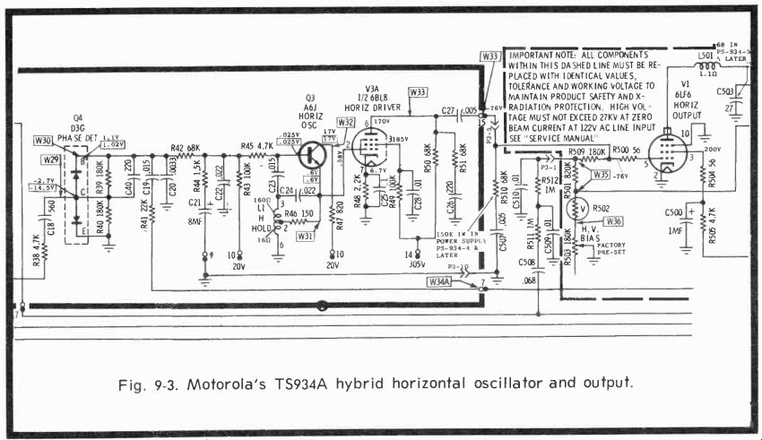
Fig. 9-3. Motorola's TS934A hybrid horizontal oscillator and output.
Later horizontal tube circuits have an output tube regulating device that is basically a pulse (and-or DC) feed from the flyback transformer through a capacitor and varistor that biases the output tube grid to keep it from going heavily positive and burning up the plate circuit should there be too heavy a high-voltage demand.
In troubleshooting this circuit, look at the oscillator frequency first. If it is working, see if its drive rate is close to 15.7 kHz; your scope can easily tell you. If the oscillator is operating on frequency, go to the rest of the circuit and look for problems there. Unfortunately, many potentials in this circuit after the 268-volt plate of the oscillator will permit the use of either AC or DC oscilloscope vertical amplifiers, but not both. So you will have to switch them manually and alternate between the two to establish AC amplitudes and waveshapes, then investigate DC potentials.
HYBRID HORIZONTAL SWEEP CIRCUITS
Hybrid horizontal sweep circuits are much like the block system shown in Fig. 9-1, and considerably simpler than the usual all-vacuum tube circuits, since AFC diodes easily supply effective correction to transistor single-stage oscillators especially with vacuum tube drivers to supply the large drives needed for the output. Why is this method used instead of all solid-state oscillators and outputs? Simply because the manufacturing process is cheaper. Does a tube horizontal output give better results? It will if the transistor output circuit doesn't have some sort of eventual regulation. The transistor isn't husky (with a good fudge factor), and there must be some means of suppressing transients. On the other hand, semiconductors are always going to last longer than tubes in most applications; therefore, they are undoubtedly more desirable.
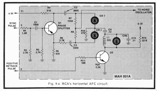
Fig. 9-4. RCA's horizontal AFC circuit.
You might notice in Fig. 9-3 the protection system using high-voltage bias (varistor R502) and the voltage divider in the grid circuit of the 6LF6 horizontal output. This is the HV pulse-type output protection and limiting circuit we've been talking about. Regulating pulses arrive between R501 and R502 from the primary of the flyback and voltage-dependent resistor R502 increases and decreases in resistance, depending on the minimum and maximum amplitude of the flyback pulses. The R502 resistance change regulates the grid conduction of the horizontal output, so excessive current is not drawn because of beam current demand. The height of the pulse is, of course, proportional to the amount of high voltage.
R503, the HV bias adjust, is set at the factory and normally does not require changing, but should be checked after oscillator, HV, or horizontal output repairs or replacement. In some other versions of this circuit, a pair of diodes is added to supply a negative cutoff potential to the output grid, insuring the tube's safety whenever the oscillator fails.
RCA Silicon Controlled Rectifier Horizontal Drive System
Although this system is several years old, it will be an RCA mainstay for a considerable period in the future. Really, all RCA 1972 solid-state chassis have this basic system, plus the CTC40, 44, and 47 receivers that preceded the CTC49, and the series of CTC54 and 46 chassis. It's a good system, a reliable one, and fundamentally simple, once you understand its operation; but understand it you must, and this sometimes takes a bit of doing. The following description is based on studies produced by Carl Moeller and Ed Milbourn, RCA senior Field Technical Services Administrators.
The horizontal AFC and oscillator circuits are contained in Module MAH. The AFC circuit is shown in Fig. 9-4. Differentiation of the combined vertical and horizontal sync pulses by C1 and R3 eliminates the former; the horizontal sync pulses are split in phase and supplied to the two inputs to the phase detector, C2 and C3. Positive retrace pulses from the flyback transformer are shaped in the collector circuit of Q3 before being applied to the common point of CR1 and CR2.
Assuming the free-running frequency of the horizontal oscillator is exactly equal to sync-pulse frequency and correctly phased, the output of the AFC circuit is zero. A tendency of the horizontal oscillator to lag the sync pulses produces a positive AFC output and, of course, if the oscillator output pulse tends to precede the sync pulse excessively, a negative AFC voltage is generated.
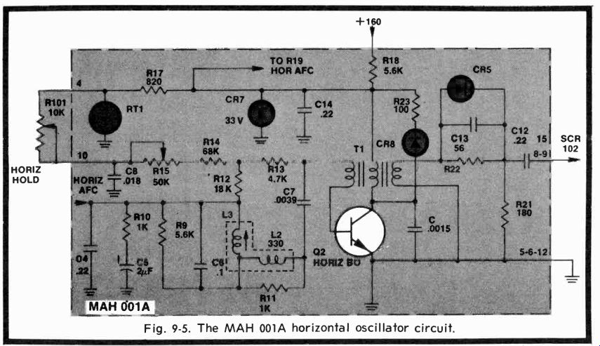
Fig. 9-5. The MAH 001A horizontal oscillator circuit.
The horizontal blocking oscillator itself is diagrammed in Fig. 9-5. Fig. 9-9 is a complete schematic of the horizontal output system, excluding the high-voltage quadrupler.
There are three resonant circuits to be considered in the operation of the yoke circuit. These are:
1. The trace resonant circuit consisting primarily of C408 and C409 in parallel. T404, the yoke, L404, and either CR101 or SCR101, whichever is conducting. The yoke inductance is by far the greatest inductance, comprising roughly 90 percent of the total. The resonant frequency of this circuit is roughly 10 kHz; therefore, the period of one-half cycle is approximately equal to the duration of one scanning interval. Refer to Fig. 9 6.
2. The retrace resonant circuit made up of C408 and C409 in parallel, T404, the yoke, L404, C413 and C414 in parallel, L104, and either CR102 or SCR102, whichever is conducting. The resonant frequency of this circuit is such that its half-cycle period is equal to retrace time. Refer to Fig. 9-7.
3. The power input resonant circuit consisting of R424 and T402 in parallel with T403, L104, and two parallel paths to ground. One of these is C412 and R407 paralleled by L406; the other is C413 and C414 in series with either SCR101 or CR101, whichever is conducting. The resonant frequency of this circuit allows the voltage at the junction of T403 and L104 to rise to its positive peak and begin to decay during each scanning interval. The precise frequency is varied by the ...
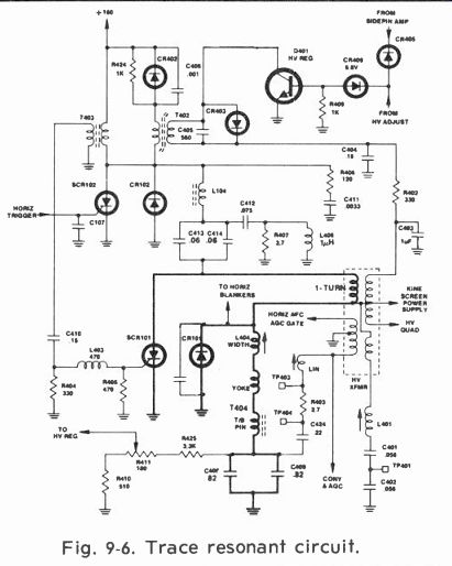
Fig. 9-6. Trace resonant circuit.
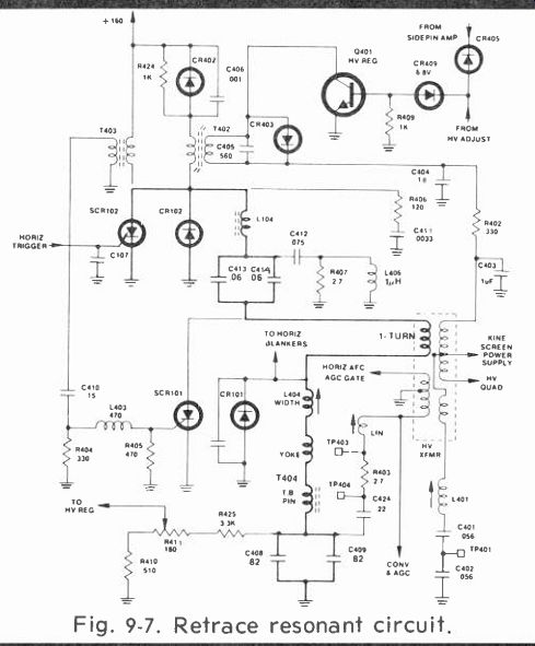
Fig. 9-7. Retrace resonant circuit.
...voltage regulator, to be explained. Current flowing through T403 generates a positive gate voltage for SCR101 during most of the scanning interval. Refer to Fig. 9-8.
Considering a point in time just after retrace is completed, time 0 in Fig. 9-10, a large current is flowing in the trace circuit and conduction is through CR101. This current decays to zero at mid-scan and reverses, flowing through SCR101 and rising from zero to maximum at the right end of scan. Near the end of the scanning interval, gate voltage is removed from SCR101, but it continues conducting.
Throughout the scan interval, the lower ends of C413 and C414 effectively are grounded. Electron current flows from ground through C413, C414, C412 and the rest of the power input circuit to B+. L104 is small compared to T403 and T402, so the voltages at its opposite ends are about the same. The voltage at the anode of SCR102 and CR102 reaches maximum slightly before the end of trace and begins to decay, since the power input circuit is resonant. Regulation of input power is accomplished by changing the resonant frequency; this is the function of the saturable reactor, T402.
When SCR102 is triggered, the retrace resonant circuit is completed and the energy stored in C412, C413, and C414 causes electron flow to continue downward through the yoke, rapidly cutting off SCR101.
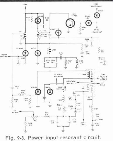
Fig. 9-8. Power input resonant circuit.
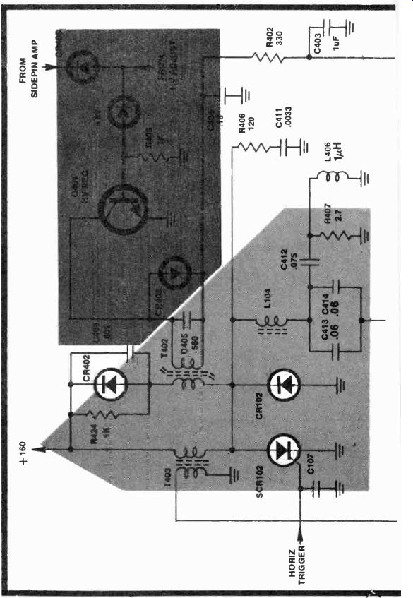
Fig. 9-9. Horizontal deflection and high-voltage regulation circuits.
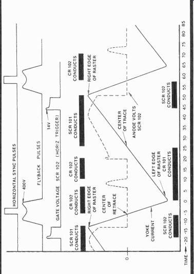
Fig. 9-10. Timing diagram of the RCA SCR horizontal deflection system.
Resonance causes the yoke current to decay to zero and reverse, cutting off SCR102 and turning on CR102. At this instant, scan is at the center of retrace. Current increases until it reaches a maximum, driving the scan to the left side of the screen, but it cannot reverse again because gate voltage no longer is present on SCR102. The large current flowing in the yoke at the end of retrace takes the only path available, through CR101. This, of course, was the condition assumed at the beginning of this summary.
The high-voltage transformer is connected parallel to the yoke circuit. During scan time either SCR101 or CR101 is conducting, thus shorting the primary so that very little energy can enter. However, during retrace the flyback voltage pulse drives the transformer primary, and the transformer converts this voltage to a higher voltage, which is used to drive the quadrupler and CRT screen power supply. Energy transfer is optimized by tuning the transformer to the third harmonic of the retrace pulse. This is the function of L401.
The Basic SCR System
A silicon controlled rectifier (SCR) is-as its name implies-a controlled rectifier fabricated from the semiconductor material, silicon. The SCR action is much like that of the thyraton tube. It is basically nonconductive until turned on by some control signal applied to a control electrode. When turned on, the device acts like a normal rectifier, and is capable of conducting high currents and exhibiting very low forward voltage drop between its anode and cathode. The SCR can be turned off by reversing the anode-cathode voltage or by reducing the current through it to the point where the SCR exhibits a high resistance.
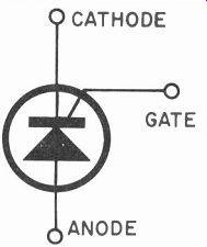
Fig. 9-11. Schematic symbol of a silicon controlled rectifier (SCR).
The SCR has three elements-an anode, a cathode and the control electrode called a gate (Fig. 9-11). When a sufficient amount of current is supplied to the gate, and the anode-cathode is forward biased, the SCR will switch on. When the anode-cathode voltage and-or current are reversed, the SCR will switch off. The amount of forward anode-cathode voltage which will result in SCR conduction depends on the gate current (Fig. 9-12). After the SCR has been switched-on, the ...
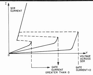
Fig. 9-12. SCR conduction and gate current relationship.
... current through it is independent of gate current. The fact that the SCR exhibits the characteristics of a switch is used to aid in the upcoming simplified description of horizontal deflection circuit operation.
The basic objective of any horizontal deflection circuit for commercial television receivers using electromagnetic deflection is the same-to cause an approximately linear current to flow in the yoke windings in such a manner as to deflect the picture tube beam from one side of the tube screen to the other (trace current). This current must be in synchronism with the video information provided in the received television signal transmission. Additionally, the yoke current must include a component which causes the picture tube beam to return to its starting position; this is, of course, the retrace or flyback current component. The basic simplified horizontal deflection waveshape and its relationship to beam scan is illustrated in Fig. 9-13.
The CTC40 chassis generates the desired horizontal deflection current with circuitry using silicon controlled rectifier devices and associated circuit elements. The essential components in the RCA CTC40 horizontal output circuit are as shown in Fig. 9-14. Essentially, diode DI and controlled rectifier SCR1 provide switching action which controls current in the horizontal yoke windings, Ly, during the picture tube beam trace interval. Diode D2 and controlled rectifier SCR2 control yoke current during the retrace interval. Components Lr, Cr, Ch, and Cy provide the necessary energy storage and timing duties. Inductance Lg, supplies a charge path for Cr and Ch from B+, thereby providing a means to "recharge" the system from the instrument power supply. Inductance Lg2 provides a gating current for rectifier SCR1 (Lg, and Lg2 comprise transformer T102). Capacitor Ch optimizes the retrace time by virtue of its resonant action with Lr.
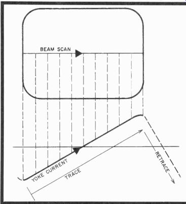
Fig. 9-13. Basic relationship between beam scan and yoke current.
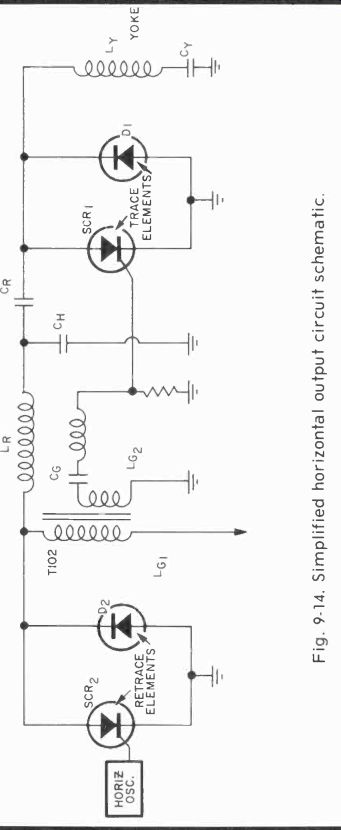
Fig. 9-14. Simplified horizontal output circuit schematic.
In order to facilitate the understanding of the operation of the horizontal output circuit, liberty has been taken to greatly simplify the circuit element illustrations in the following discussion. In Fig. 9-15 (and the illustrations following), trace elements SCR1 and D1 together comprise an SPST switch labeled S1. Retrace elements SCR2 and D2 comprise another SPST switch labeled S2. The relationship of the yoke current waveshape and the beam trace-retrace also is illustrated in Fig. 9-15.
Trace time: Referring to Fig. 9-16, during the first half of trace time (T to T2 ), switch S1 is closed, allowing a field previously produced about the yoke inductance, Ly, to collapse, resulting in a current which charges capacitor Cy.
This yoke current causes the picture tube beam to deflect to approximately the middle of the screen. During the second half of the trace time interval T2 to T5 the current in the yoke circuit reverses because the capacitor Cy now discharges back into the yoke inductance, Ly (Fig. 9-17). This current causes the picture tube beam to complete its trace.
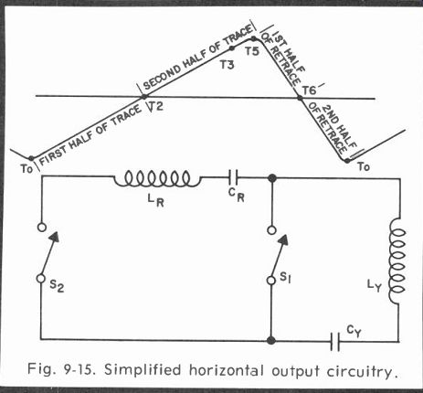
Fig. 9-15. Simplified horizontal output circuitry.
Retrace initiation: However, at time T3 (Fig. 9-18) a pulse from the horizontal oscillator causes switch S2 to close, releasing a previously stored charge on Cr. The resulting current flows in the circuit as illustrated in Fig. 9-18. Because of the natural resonance of Lr and Cr, this resonant current ...
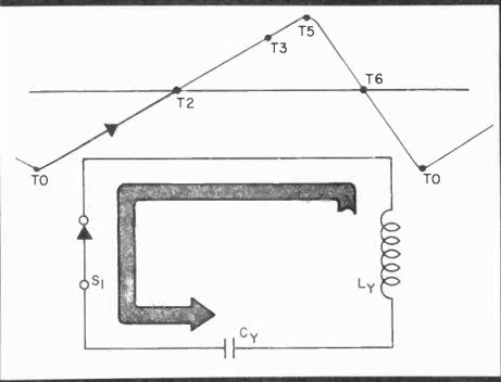
Fig. 9-16. Circuit current T0 to T2; the first half trace yoke field collapses
into Cy.
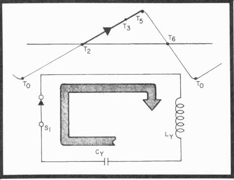
Fig. 9-17. Circuit current T2 to T5; during the second half of the trace,
Cy discharges into the yoke windings.
...becomes equal to the yoke current at T5 . At this time S1 opens, S2 remains closed, and retrace starts.
Retrace: The simplified retrace circuit with Sz closed and Si open is shown in Fig. 9-19. Basically, Lr, Cr, Cy, and Ly are connected in series. The natural resonant frequency of this circuit is much greater than that of the yoke circuit, Ly and Cy. As a result, the current change through the yoke windings Ly during retrace time is much faster than that during trace time. This, of course, causes the picture tube beam to retrace (flyback) very rapidly.
During the first half of the retrace time (T5 to T6 , Fig. 9 19 ), the retrace yoke current flows in the direction as shown at time T6 ; however, the retrace circuit current reverses because of resonant circuit action (Fig. 9-20), and the last half of the retrace action occurs (T6 to T0 ).
At time T0 , switch S1 closes and shortly thereafter S2 opens. The field about the yoke inductance starts to collapse, and the resulting current again starts the trace interval. The trace-retrace cycle now has been completed. Fig. 9-21 illustrates the trace and retrace waveforms.
ZENITH'S CERAMIC THICK FILM MODULE
Zenith is not only moving rapidly forward with monolithic ICs, but also with thick film complex circuits-sometimes ...
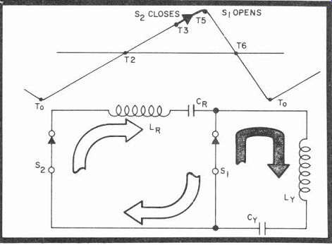
Fig. 9-18. Circuit current (T2 to T5) during retrace initiation.
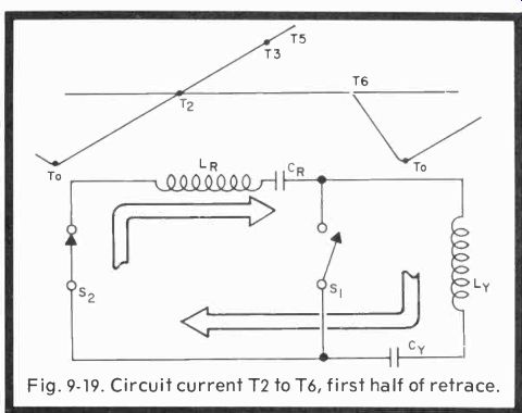
Fig. 9-19. Circuit current T2 to T6, first half of retrace.
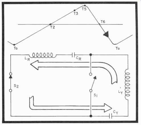
Fig. 9-20. Circuit current T6 to T0, second half of retrace.
...intermixed, as shown in Fig. 9-22. Here, we have a thick film resistor matrix module for the chroma subcarrier, a thick film vertical module, and the horizontal AFC and oscillator module. What's happening in these circuits is that Zenith is more or less substituting transistor chips and thick film modules for the individual transistors and discrete passive components that formerly constituted either part of or the entire module. Fig. 9-23 is a schematic of the original horizontal Duramodule used in the 40BC50, Zenith's first all-solid state receiver, while Fig. 9-24 is the schematic of the actual thick film circuit that supplants it. Don't be confused by symmetrical D1-D2 on the schematic; they're just CR801 and 802 on the Duramodule. Also, Q4 is sawtooth shaper Q804, Q1 is Q801, Q2 is Q802, and Q803 is Q3 turned around. So here, in stead of pulling a transistor or two when the oscillator fails, you'll be able to exchange an entire module at a single pull and insertion, and any oscillator fault will be repaired. Say you'd like to replace just a single transistor instead? Sorry, but that's the way the industry's going-to throwaways, pretty fast and furiously.
Let's go back to the original horizontal Duramodule (Fig. 9-23) and see how it works. Sawtooth shaper Q804 receives a negative-going pulse on the emitter that sends the transistor into conduction, discharging C803 to sharpen the initial leading edge of the incoming waveform, then charging through R812 to form the remainder of the sawtooth. The negative part of this sawtooth will appear across R802, since it is coupled there by C802, but the waveform will not drop across R803 because CR802 has been turned on to place a short across R803. The reverse occurs when the positive part of the sawtooth places a short across R802 because of the conduction of CR801.
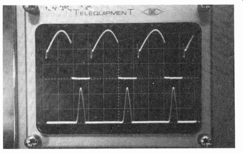
Fig. 9-21. Trace (top) and retrace waveforms for RCA's SCRs. Top trace is
100v per division, while the bottom trace is 200v per division. Time base
is 20 microseconds per division.
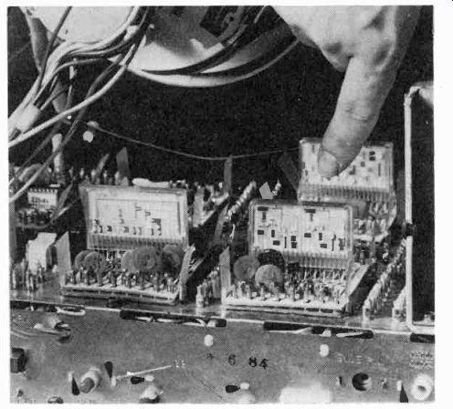
Fig. 9-22. Rear chassis view, showing thick film hybrid circuits serving
as the horizontal, vertical, and subcarrier regenerator in Zenith's 25CC55
receivers.
If the incoming negative sync pulse arrives at the common cathodes during crossover time, both diodes go into full conduction for an equal time and-or one is completely on and the other completely off. Therefore, the outputs will cancel, leaving nothing. However, should sync pulses lag or lead the sawtooth ramp, one diode will conduct for a shorter or longer period than the other, and the difference output will be positive or negative, depending on the difference in conduction times.
C806 and R806 form an anti-hunt network to protect against overreaction at warmup.
The diode DC output makes Q801 act as a variable resistance, changing the charge potential on C809, which is in series with L214, the horizontal hold tunable inductance. Q802 is a self-starting oscillator because of forward bias coming from the 125-volt line through T7 and resistors R813 and R816.
The load resistor is R818.
You may see no apparent source of collector voltage for Q801. AC sinewaves generated by the horizontal oscillator go back through All to C809. Here, these voltages are rectified by CR803 and form the supply voltage for the AFC. The oscillator output is now large enough in amplitude and sufficiently shaped that it will drive the Q803 horizontal driver completely into saturation and cutoff, so that its drive voltage, coupled through T206 to the horizontal output transistor, is the square-wave voltage that's needed for adequate off-on drive.
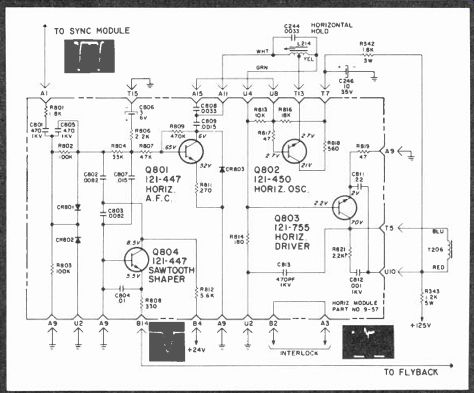
Fig. 9-23. Schematic of Zenith's original horizontal I Duramodule used in
the 40BC50 receiver chassis.
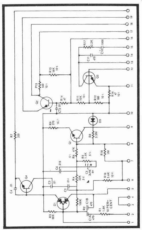
Fig. 9-24. Schematic of Zenith's thick film horizontal module that replaces
many discrete portions of the Duraniodule shown in Fig. 9-23.
QUESTIONS
1. Why are AFC diode circuits so critical?
2. What is the greatest dissipation time factor in horizontal output stages?
3. What is 263 times faster than vertical sync, and why?
4. Are there any horizontal sweep systems without dampers, HV regulators, tube rectifiers, unshielded flyback transformers?
5. What are anti-hunt networks and where are they used?
6. What function has the R44-C21 time constant in Fig. 9-3?
7. The horizontal output tube cuts en at what point of the driving waveform?
8. What does a varistor do n a horizontal output tube protection system?
9. What are the three resonant circuits in an SCR drive system?
10. Are HV transformers connected in series or parallel with the deflection yoke?
11. How can an SCR be turned off?
12. Silicon controlled rectifiers are peculiar beasts. They can be turned by a gate pulse, but now do you stop conduction?
13. In Fig. 9-21, retrace (top) and trace waveforms (bottom), are shown at 20 microseconds per div. and 200v p-p. Which SCR conducts longer and why?
Next: Link | --HV Supplies & Pincushion Circuits
Also see:
TV Antennas and Transmission lines
Air Time--An Intro to Television Broadcasting