Digital audio recording and reproduction (playback) processors serve as input and output transducers to the digital domain. They convert an analog audio waveform into a signal suitable for digital processing, storage, or transmission, and then convert the signal back to analog form for playback. In a linear pulse-code modulation (PCM) system, the functions of the reproduction circuits are largely reversed from those in the record side. Reproduction functions include timebase correction, demodulation, demultiplexing, error correction, digital-to-analog (D/A) conversion, output sample-and-hold (S/H) circuit, and output lowpass filtering. Oversampling digital filters, preceding D/A conversion, are used universally.
Reproduction Processing
The reproduction signal chain accepts a coded binary signal and ultimately reconstructs an analog waveform, as shown in Fgr. 1. The reproduction circuits must minimize any detrimental effects of data storage or transmission. For example, storage media suffer from limitations such as mechanical variations and potential for physical damage.
With analog storage, problems generally must be corrected within the medium itself; For example, to minimize wow and flutter, a turntable's speed must be precise. With digital systems, the potential for degradation is even greater.
However, digital processing offers the opportunity to correct many faults. For example, the reproduction circuits buffer the data to minimize the effects of timing variations in the data, and also perform error correction.
To achieve high data density, the physical fidelity of the stored or transmitted channel code waveform is allowed to deteriorate. Thus, the signal does not have the clean characteristics that the original data may have enjoyed. For example, a recorded digital signal as read from a magnetic-disk head is not sharply delineated, but instead is noisy and rounded from bandlimiting. A waveform shaper circuit identifies the transitions and reconstructs a valid data signal. In this way, data can be recovered without penalty for the waveform's deterioration.
Synchronization pulses and other clocking information in the bitstream are identified and used by timebase correction circuits to synchronize the playback signal, delineate individual frames, and thus determine the binary content of each pulse. In most cases, the signal contains timing errors such as jitter as it’s received for playback.
Phase-locked loops (PLLs) and data buffers can overcome this problem. A buffer can be thought of as a pail of water:
water is poured into the pail carelessly, but a spigot at the bottom of the pail supplies a constant stream. Specifically, a buffer is a memory into which the data is fed irregularly, as it’s received. However, data is clocked from the buffer at an accurately controlled rate, ensuring precise data timing. Samples can be reassembled at the same rate at which they were taken. Timebase correction is discussed in more detail later in this Section .
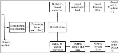
FGR. 1 A conceptual linear PCM reproduction Section .
In practice, digital oversampling filters are used.
The modulated audio data, whether it’s eight-to-fourteen modulation (EFM), modified frequency modulation (MFM), or another code, is typically demodulated to nonreturn to zero (NRZ) code, that is, a simple code in which the amplitude level represents the binary information. The audio data thus regains a readily readable form and is ready for further reproduction processing. In addition, demultiplexing is performed to restore parallel structure to the audio data. The demultiplexer circuit accepts a serial bit input, counting as the bits are clocked in. When a full word has been received, it outputs all the bits of the word simultaneously, to form parallel data.
The audio data and coded error-correction data are identified and separated from other peripheral data. Using the error-correction data, the data signal is checked for errors that may have occurred following encoding. Because of the data density used in digital recording and transmission, many systems anticipate errors with certainty;
only their frequency and severity vary. The error-correction circuits must de-interleave the data. Prior to recording, the data is scattered in the bitstream to ensure that a defect does not affect consecutive data. With de-interleaving, the data is properly reassembled in time, and errors caused by intervening defects are scattered through the bitstream, where they are more easily corrected. The data is checked for errors using redundancy techniques. When calculated parity does not agree with parity read from the bitstream, an error has likely occurred in the audio data. Error correction algorithms are used to calculate and restore the correct values. If within tolerance, errors can be detected and corrected with absolute fidelity to the original data, making digital recording and transmission a highly reliable technique. If the errors are too extensive for correction, error concealment techniques are used. Most simply, the last data value is held until valid data resumes.
Alternatively, interpolation methods calculate new data to form a bridge over the error. A more complete discussion of error correction techniques can be found in Section 5. The serial bitstream consists of the original audio data, or at least data as close to the original as the error correction circuitry has yielded. On leaving the reproduction processing circuitry, the data has regained timing stability, been de-multiplexed, been de-interleaved, and incurred errors have been corrected. The data is ready for digital-to analog conversion. Digital filtering, which precedes D/A conversion, is discussed later in this Section.
Digital-to-Analog Converter
The digital-to-analog (D/A) converter is one of the most critical elements in the reproduction system. Just as the analog-to-digital (A/D) converter largely determines the overall quality of the encoded signal, the D/A converter determines how accurately the digitized signal will be restored to the analog domain. The task of D/A conversion demands great precision; For example, with a ±10-V scale, a 16-bit converter will output voltage steps that measure 0.000305 V, and a 24-bit converter must output steps that measure only 0.00000119 V. Traditional D/A converters can exhibit nonlinearity similar to that of A/D converters; sigma-delta converters, operating on a time basis rather than an amplitude basis, can overcome some deficiencies but must use noise shaping to reduce the in-band noise floor. Fortunately, high-quality D/A converters are available at low cost.
Traditional D/A converters process parallel data words and are prone to many of the same errors as A/D converters, as described in Section 3. In practice, resolution is chiefly determined by absolute linearity error and differential linearity error. Absolute linearity error is a deviation from the ideal quantization staircase and can be measured at full signal level; it’s smaller than ±1/2 LSB (least significant bit). Differential linearity error is a relative deviation from the ideal staircase by any individual step.
The error is uncorrelated with high signal levels but correlated with low signal levels; as a result it’s most apparent at low signal levels as distortion.
Differential nonlinearity appears as wide and narrow codes, and can cause entire sections of the transfer function to be missing. Differential nonlinearity is minor with high-amplitude signals but the errors can dominate low level signals. For example, a signal at -80 dBFS (dB Full Scale) will pass through only six or seven codes in a 16-bit quantizer; if half of those codes are missing, the result will be 14-bit performance. Depending on bias, the differential linearity error in a 16-bit D/A converter for a -90 dBFS sine wave signal can result in generated levels ranging from -85.9 dB to -98.2 dB. Because the bits and their associated errors switch in and out throughout the transfer function, their effect is signal dependent. Thus, harmonic and intermodulation distortion and noise vary with signal conditions. Because this kind of error is correlated with the audio signal, it’s more readily perceived. Nonmonotonicity is an extreme case of nonlinearity; an increase in a particular digital code does not result in an increase in the output analog voltage; most converters are guaranteed against this.
A linearity test measures the converter's ability to record or reproduce various signals at the proper amplitude.
Specifically, linearity describes the converter's ability to output an analog signal that directly conforms to a digital word. For example, when a bit changes from 1 to 0 in a D/A converter, the analog output must decrease exactly by a proportional amount. Any nonlinearity results in distortion in the audio signal; the amount that the analog voltage changes will depend on which bit has changed. Every PCM digital word contains a series of binary digits, arranged in powers of two. The most significant bit (MSB) accounts for a change in fully half of the analog signal's amplitude, and the least significant bit accounts for the least change , for example, in an 18-bit word, an amplitude change of less than four parts per million. Physical realities conspire against this accuracy. Traditional ladder converters exhibit differential nonlinearity because of bit weighting errors; thermal or physical stress, aging, and temperature variations are also factors.
To help equipment manufacturers use D/A converters to their best advantage, some ladder D/A chips provide a means to calibrate the converter. Consider a 16-bit D/A converter offering calibration of the MSB. Because the MSB is so much larger than the other bits, an MSB error of only 0.01% (one part in 10,000) would completely negate the contributions of the two LSBs (which account for one part in 21,845 of the total signal amplitude). An error of 0.1% in the MSB would swamp the combined values of the five smallest bits. Overall, the tolerance of the MSB in a 16 bit converter is 1/65,536 of the LSB. Some converters offer calibration of the four most significant bits. It’s interesting to note that fully 93% of the total analog output is represented through these four most significant bits. These MSBs largely steer the converter's output amplitude; when they are properly calibrated, the entire output signal of a well-designed D/A converter will be more accurate. This accuracy is most significant at low levels, usually below -60 dBFS. As noted, any nonlinearity in D/A conversion will be apparent as a deviation from nominal amplitude. Moreover, such nonlinearity can be heard; for example, by using a test disc containing a dithered fade to silence tone, poor D/A linearity is clearly audible.
The low-level performance of D/A converters can be evaluated using tests for D/A linearity. For example, Fgr. 2 shows a D/A converter's low-level linearity. Reproduced signals lower than -100 dBFS in amplitude show nonlinearity. For example, a -100-dBFS signal is reproduced at an amplitude of -99 dBFS, and a -110 dBFS signal is reproduced at approximately -105 dBFS.
Depending on signal conditions, this kind of error in low level dynamics might audibly alter low-amplitude information.
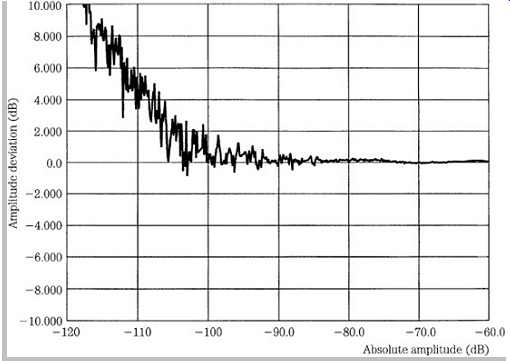
FGR. 2 An example of a low-level linearity measurement of a D/A converter
showing increasing nonlinearity with decreasing amplitude.
In practice, linear 16-bit conversion is insufficient for 16 bit data. Converters must have a greater dynamic range than the audio signal itself. No matter how many bits are converted, the accuracy of the conversion, and hence the fidelity of the audio signal, hinges on the linearity of the converter. Linearity errors in converters generally result in a stochastic deviation; it varies randomly from sample to sample. However, relative error increases as level decreases. The linearity of a D/A converter, and not the number of bits it uses, measures its accuracy.
A D/A converter must have a fast settling time. Settling time for a D/A converter is the elapsed time between a new input code and the time when the analog output falls within a specified tolerance (perhaps ±1/2 LSB). The settling time can vary with the magnitude of change in the input word.
Most D/A converters operate with a two's complement input. For example, an 8-bit D/A converter would have a most positive value of 01111111 and a most negative value of 10000000. In this format the MSB is complemented to serve as a sign bit. To accomplish this, the MSB can be inverted before the word is input to the D/A converter, or the D/A converter might have a separate, complementing input for the MSB.
Digitally generated test tones are often used to measure D/A converters; it’s important to choose test frequencies that are not correlated with the sampling frequency.
Otherwise, a small sequence of codes might be reproduced over and over, without fully exercising the converter. Depending on the converter's linearity at those particular codes, the output distortion might measure better, or worse, than typical performance. For example, when replaying a 1-second, 1-kHz, 0-dBFS sine wave sampled at 44.1 kHz, only 441 different codes would be used over the 44,100 points. A 0-dBFS sine wave at 997 Hz would use 20,542 codes, giving a much better representation of converter performance. Standard test tones have been selected to avoid this anomaly. For example, some standard test frequencies are: 17, 31, 61, 127, 251, 499, 997, 1999, 4001, 7993, 10,007, 12,503, 16,001, 17,989, and 19,997 Hz.
Weighted-Resistor Digital-to-Analog Converter
Various types of D/A converters are used for audio digitization. Operation of traditional converters is quite different from sigma-delta converters. The former are more easily understood; we begin with an illustration of the operation of a traditional ladder D/A converter. A D/A converter accepts an input digital word and converts it to an output analog voltage or current. The simplest kind of D/A converter, known as a weighted-resistor D/A converter, contains a series of resistors and switches, as shown in Fgr. 3.
A weighted-resistor converter contains a switch for each input bit; the corresponding resistor represents the binary value associated with that bit. A reference voltage generates current through the resistors. A digital 1 closes a switch and contributes a current, and a digital 0 opens a switch and prevents current flow. An operational amplifier sums the currents and converts them to an output voltage. A low-value binary word with many 0s closes few switches thus a small voltage results. A high-value word with many 1s closes many switches; thus, a high voltage results.
Consider this example of an 8-bit converter:
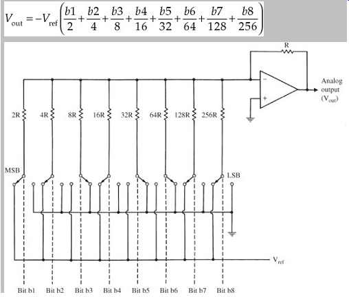
FGR. 3 A weighted-resistor D/A converter uses resistors related by powers
of 2, which limits resolution.
where b1 through b8 represent the input binary bits. For example, suppose the reference voltage Vref = 10 V and the input word is 11010011:

Although this weighted-resistor design looks good on paper, it’s rarely used in practice because of the complexity in manufacturing resistors with sufficient accuracy. It’s extremely difficult to manufacture precise resistor values so that each next resistor value is exactly a power of 2 greater than the previous one. For example, in a 16-bit D/A converter, the largest-to-smallest ohm (O) resistor ratio is 65,536:1. If the smallest resistor value is 1 k-ohm, the largest is over 65 MO. Similarly, the smallest current might be 30 nA (nanoampere) and the largest 2 mA (milliampere). In short, this design demands manufacturing conditions that cannot be efficiently met.
R-2R Ladder Digital-to-Analog Converter
A more suitable design approach for a D/A converter is the R-2R resistor ladder, as shown in Fgr. 4. This circuit contains resistors and switches; in particular, there are two resistors per bit. Each switch contributes its appropriately weighted component to the output. The current splits at each node of the ladder, resulting in current flows through the switch resistors that are weighted by binary powers of 2. If current I flows from the reference voltage, I/2 flows through the first switch, I/4 through the second switch, I/8 through the third switch, and so on. Digital input bits are used to control ladder switches to produce an analog output. For example:
With Vref = 10 V and an input word of 01010110:

The R-2R network can be efficiently manufactured; only two values of resistors are needed. As noted, in many converters, one or several MSBs can be calibrated to improve linearity. In some designs, stability with respect to temperature is achieved with a compensation feedback loop. A high-precision signal is generated and compared to the signal generated by the D/A converter. The difference between the two is applied to a memory, which in turn outputs a correction word to the input of the D/A converter. Errors caused by variations in the components are thus self-corrected and distortion is minimized.
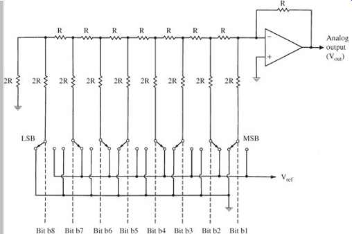
FGR. 4 An R-2R D/A converter uses only two resistor values, improving resolution.
Zero-Cross Distortion
A quality D/A converter must be highly accurate. As noted, a 16-bit D/A converter with an output range of ±10 V has a difference between quantization levels of 20/65,536 = 0.000305 V. For example, the output from the input word 1000 0000 0000 0000 should be 0.3 mV larger than that from the input word 0111 1111 1111 1111. In other words, the sum of the lower 15 bits must be accurate to that precision, compared to the value of the highest bit. The lower 15 bits should have a relative error of one-half quantization level, as should the MSB. However, differential linearity error is greatest for the MSB, which produces the largest output voltage. Moreover, the MSB changes each time the output waveform passes through zero. Difficulty in achieving accuracy at the center of a ladder D/A converter's range leads to zero-cross distortion.
Zero-cross distortion occurs at the zero-cross point between the positive and negative polarity portions of an analog waveform. When a resistor ladder D/A converter is switched around its MSB, that is, from 1000 0000 0000 0000 to 0111 1111 1111 1111 to reflect a polarity change, the internal network of resistors must be switched. Current fluctuations and variations in bit switching speeds can conspire to create differential nonlinearity and glitches, as shown in Fgr. 5. Collectively, these defects are known as zero-cross distortion. Because musical waveforms continually change (twice each cycle) between positive and negative polarity, the zero axis is crossed repeatedly as the MSB is turned on and off. The error is particularly troublesome when reproducing low-level signals because the fixed-amplitude glitch may be proportionally large with respect to the signal. Furthermore, the audibility of zero cross distortion can be aggravated by dithering because of the increase in the number of transitions around the MSB.
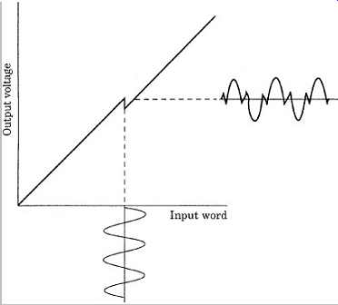
FGR. 5 Crossover distortion occurs at the zero-cross point when the input
word of a D/A converter changes polarity, resulting in a glitch in the output
waveform.
Ideally, when there is no error difference between the smallest and largest resistors in the ladder, there is no output error. However, the MSB generally has large error compared to the LSB; the error can be larger than the value of the LSB itself. This is because the MSB in a 16-bit converter must be represented by a current value with an accuracy greater than 1/65,536 of the LSB. (This demonstrates why adjustment of the MSB is paramount in achieving converter linearity.) Similarly, error can occur when the 2nd, 3rd, and 4th bits are switched; however, the error proportionally decreases as the signal level increases. By the same token, error is relatively greatest for low-level audio signals. When longer word-length converters are used, it’s proportionally difficult to match resistor values.
Zero-cross distortion can be alleviated by careful calibration of the converter's most significant bits.
Alternatively, a sign-magnitude configuration can be used; the output amplifier switches between each positive and negative input code excursion. As a result, the LSB toggles around bipolar-zero, minimizing zero-cross distortion. Zero cross distortion can also be reduced by providing a complementary D/A converter for each waveform polarity.
Sign-magnitude code values are supplied to both parallel converters. In this way, total switching of digits across bipolar-zero never occurs. Zero-cross distortion is not present in sigma-delta D/A converters, as described in Section 18.
High-Bit D/A Conversion
Many manufacturers use D/A converters with 18-, 20- or 24-bit resolution in reproduction systems to provide greater playback fidelity for 16-bit recordings. The rationale for this lies in flaws that are inherent in D/A converters. Except in theory, 16-bit converters cannot fully decode a 16-bit signal without a degree of error. When , for example, 18 bits are derived from 16-bit data and converted with 18-bit resolution, errors can be reduced and reproduction specifications improved. To realize the full potential of audio fidelity, the signal digitization and processing steps must have a greater dynamic range than the final recording.
The choice of 16-bit words for the CD and other formats was determined primarily by the availability of 16-bit D/A converters and the fact that longer word lengths diminish playing time. However, 18-bit converters , for example, can provide better conversion of the stored 16 bits. When done correctly, 18-bit conversion improves amplitude resolution by ensuring a fully linear conversion of the 16-bit signal. An 18-bit D/A converter has 262,144 levels, exactly four times as many output levels as a 16-bit converter. Any nonlinearity is correspondingly smaller, and increasing the quantization word length at the conversion stage results in an increase in signal-to-noise (S/N) ratio. Simultaneously, any quantization artifacts are diminished. In other words, in this example, an 18-bit D/A converter gives better 16-bit conversion. In fact, the two extra bits of a linear 18-bit converter don’t have to be connected to yield improved 16-bit performance.
The intent of high-bit D/A converters can be compared to that of oversampling: while the sampling frequency is increased, the method does not create new information; it makes better use of existing information. Oversampling provides the opportunity for high-bit conversion of 16-bit data. When a 44.1-kHz, 16-bit signal is oversampled, both the sampling frequency and number of bits are increased- the former because of oversampling, and the latter because of filter coefficient multiplication. The digital filter must be appropriately designed so the output word contains useful information in the bits below the 16-bit level.
It’s not meaningful to gauge the performance of a D/A or A/D converter by its word length. More accurately, the S/N ratio measures the ratio between the maximum signal and the noise in the absence of signal. Because systems mute the output when there is a null signal, low-level error is removed. A dynamic range measurement is more useful when measured as the ratio of the maximum signal to the broadband noise (0 Hz to 20 kHz) using a -60-dBFS signal. This provides a measure of low-level distortion.
Using the dynamic range measurement, a converter's ENOB (effective number of bits) can be calculated:

For example, a 16-bit converter with a dynamic range of 90 dB provides 14.7 bits of resolution; 1.3 bits are mired in distortion and noise.
In many designs, sigma-delta D/A converters are used.
They minimize many problems inherent in traditional converter design. Sigma-delta systems use very high over-sampling rates, noise shaping, and one- or multi-bit conversion. A true one-bit system outputs a binary waveform, at a very high rate, to represent the audio waveform. Other multi-bit systems output a multi-value step signal that forms a pulse-width modulation (PWM) representation of the audio signal. Because of inherently high noise levels, sigma-delta systems must use noise shaping algorithms. Sigma-delta conversion is discussed in Section 18.
Although sigma-delta converters are widely used, traditional converters can offer some advantages. Because traditional converters don’t employ noise shaping, they don’t yield high out-of-band noise. In addition, at very low signal levels, the binary-weighted current sources are not heavily switched, so noise and glitching artifacts are very low.
Output Sample-and-Hold Circuit
Many digital audio systems contain two sample-and-hold (S/H) circuits. One S/H circuit at the input samples the analog value and maintains it while A/D conversion occurs.
Another S/H circuit on the output samples and holds the signal output from the D/A converter, primarily to remove irregular signals called switching glitches. Because it can also compensate for a frequency response anomaly called aperture error, the output S/H circuit is sometimes called the aperture circuit.
Many D/A converters can generate erroneous signals, or glitches, which are superimposed on the analog output voltage. Digital data input to a D/A converter may require time to stabilize to the correct binary levels. In particular, in some converters, input bits might not switch states simultaneously. For example, during an input switch from 01111111 to 10000000, the MSB might switch to 1 before the other bits; this yields a momentary value of 11111111, creating an output voltage spike of one-half full scale. Even D/A converters with very fast settling times can exhibit momentary glitches. If these glitches are allowed to proceed to the digitization system's output, they are manifested as distortion.
An output S/H circuit can be used to deglitch a D/A converter's output signal. The output S/H circuit acquires voltage from the D/A converter only when that circuit has reached a stable output condition. That correct voltage is held by the S/H circuit during the intervals when the D/A converter switches between samples. This ensures a glitch free output pulse-amplitude modulation (PAM) signal. The operation of an output S/H circuit is shown in Fgr. 6.
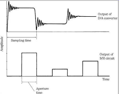
FGR. 6 An output S/H circuit can be used to remove glitches in the signal
output from some D/A converters.
From a general hardware standpoint, the output S/H circuit is designed similarly to the input S/H circuit. In some specifications, such as droop, the output S/H circuit might be less precise. Any droop results in only a dc shift at the digitization system's output, and this can be easily removed. In other respects, the output S/H circuit must be carefully designed and implemented. Because of its differing utility, the output S/H circuit requires attention to specifications such as hold time and transition speed from sample to sample.
The S/H circuit is occasionally used to correct for aperture error, an attenuation of high frequencies. Different approaches can also be used. Aperture error stems from the width of the output samples. In this case, the narrower the pulse width, the less the aperture error. Given ideal (instantaneous) A/D sampling, the output of an ideal D/A converter would be an impulse train corresponding to the original sample points; there would be no high-frequency attenuation. However, an ideal D/A converter is an impossibility. The PAM staircase waveform comprises pulses each with a width of one sample period.
(Mathematically, the function is a convolution of the original samples by a square pulse with width of one sample period.) The spectrum of a series of pulses of finite width naturally attenuates at high frequencies. This differs from the original flat response of infinitesimal pulse widths; thus, a frequency response error called aperture error results, in which high audio frequencies are attenuated. Specifically, the frequency response follows a lowpass sin(x)/x function.
When the output pulse width is equal to the sample period, the frequency response is zero at multiples of the sampling frequency, as shown in Fgr. 7A. The attenuation of the in band high-frequency response and that of high-frequency images can be observed.
At the Nyquist frequency, the function's value is 0.64, yielding an attenuation of 3.9 dB. This can be addressed with S/H circuits by approximating the impulse train output from an ideal D/A converter; the duration of the hold time is decreased in the S/H circuit. Sampling theory demonstrates that the bandwidth of the response is determined by the pulse width. The shorter the duration of the pulse, the greater the bandwidth. Specifically, if the output pulse width is narrowed with a shorter hold time, the attenuation at the half-sampling frequency can be decreased, as shown in Fgr. 7B, where the pulse width is halved. If hold time is set to one-quarter of a sample period, the amplitude at the Nyquist frequency is 0.97, yielding an attenuation of 0.2 dB. This is considered optimal because a shorter hold time degrades the S/N ratio of the system.
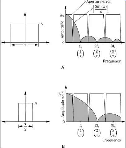
FGR. 7 Aperture error can be minimized by decreasing the output pulse width.
A. A pulse width equal to the sample period yields an in-band high-frequency
attenuation. B. In band high-frequency response improves when pulse width is
one-half the sample period.
Another remedy for aperture error is frequency compensation of the data prior to D/A conversion; this can be built into the digital lowpass filter that precedes the S/H circuit. This high-frequency boost, offset by aperture error, produces a net flat response, and the S/N ratio is not degraded. A boost could also be designed into the succeeding analog lowpass filter. Alternatively, a pre emphasis high-frequency boost could be applied at the system input; the naturally occurring de-emphasis at the output S/H circuit would result in a flat response.
When an output S/H circuit is used to eliminate switching errors caused by the D/A converter during transition, the S/H circuit must avoid introducing transition errors of its own. An S/H circuit outputs a steady value while in the hold mode. When switching to the sample (or acquisition) mode, a slow transition introduces incorrect intermediate values into the staircase voltage. This problem is extraneous in the input S/H circuit because the A/D converter accomplishes its digitization during the hold mode and ignores the transition mode. However, the output S/H circuit is always connected to the system output and any transition error appears at the output. In other words, not only are the levels themselves part of the output signal, but the way in which the S/H circuit moves from sample to sample is included as well.
Distortion is greatest for high frequencies because they have a large difference between values. For example, with a 48-kHz sampling frequency, a 20-Hz signal does not change appreciably in one sampling interval; however, a high-level 20-kHz signal will traverse almost the full amplitude range. Although the distortion products themselves can be removed by the output filter, these products can internally beat with the sampling frequency to generate in-band distortion as well. To overcome this problem, the output S/H circuit must switch as quickly as possible from hold to sample mode. A square-wave response would be ideal.
In theory, this eliminates the possibility of distortion caused by transition; however, in practice, it’s impossible to achieve the necessary high slew rate, calculated to be as high as 5 V/ns (volts per nanosecond). Thus, an additional modification to the basic S/H circuit can be applied. An exponential change in amplitude from one quantization interval to the next does not create nonlinearity in the signal.
Following output filtering, this exponential acquisition results in a linear response. It can be shown that an exponential transition from sample to sample causes only a slight high-frequency de-emphasis at the output, but no distortion or nonlinearity. An S/H circuit that integrates the difference between its present and next value yields such an exponential transition. The attenuation of high frequencies in an integrate-and-hold circuit is less than that produced by the sample-and-hold process itself, and also can be equalized.
The output S/H circuit thus removes switching glitches from the D/A converter's output voltage. Hold time can be set to less than a sample period to minimize aperture error.
Many D/A converters are stringently designed to avoid switching glitches, and thus operate without an S/H circuit; aperture error is corrected in the digital filter. In some cases, the S/H function is included in the D/A converter chip. Whichever method is used, the PAM staircase analog signal is ready for output filtering, and final reconstruction.
Output Lowpass Filter
The first and last circuits in an audio digitization system are lowpass filters, known as anti-aliasing and anti-imaging filters, respectively. Although their analog designs can be almost identical, their functions are very different. In lieu of classic analog anti-imaging filters, digital filters using oversampling techniques have replaced brick-wall analog filters. However, even digital filters employ a low-order analog lowpass filter on the final output of the system.
Given the criteria of the Nyquist sampling theorem, the function of the input low-pass filter is clear: it removes all frequency content above the half-sampling frequency to prevent aliasing. Similarly, a lowpass filter at the output of the digitization system removes frequency content above the half-sampling frequency. However, its function is different. This filter converts the D/A converter's output pulse-amplitude modulation (PAM) staircase to a smoothly continuous waveform, thus reconstructing the bandlimited input signal. The PAM staircase is an analog waveform, but it contains modulation artifacts of the sampling process that create high-frequency components not present in the original signal. An output lowpass filter converts the staircase into a smoothly continuous waveform by removing the high-frequency components, leaving the original waveform. The staircase signal is smoothed; the output filter is sometimes called a smoothing filter.
The conceptual design criteria for an analog output lowpass filter are similar to those of the input filter. The passband should be flat and the stopband highly attenuated. The cutoff slope should be steep. Audibility of any phase shift must be considered. One criteria unique to output lowpass filters is transient response. Unlike the input filter, it must process the amplitude changes in the staircase waveform. Just as a slow output S/H circuit can introduce distortion, the output filter can create unwanted byproducts if its transient response is inadequate. One consideration not commonly addressed is the possible presence of extreme high-frequency components of several megahertz that might be contained in the output signal.
Because of its high-speed operation, digital processing equipment can create this noise, and the filtering characteristics of some audio lowpass filters don’t extend to those frequencies.
Viewing the output filtering process from a more mathematical standpoint, we can observe how sampling creates the need for filtering. Sampling multiplies the time domain audio signal with the time domain sampling (pulse) signal. In terms of the spectra of these two sampled signals, this convolution produces a new sampled spectrum identical to the original unsampled spectrum. However, additional spectra are infinitely repeated across the frequency domain at multiples of the sample frequency. For example, an original 1-kHz sine wave sampled at 48 kHz also creates components at 47, 49, 95, 97 kHz, and so on.
Although the sample-and-hold process substantially reduces the amplitude of the extraneous frequency bands, significant components still remain after the S/H circuit, particularly in the region near the audio band (see Fgr. 7).
To convert the sampled information back into correct analog information, the image spectra must be removed, leaving only the original baseband spectrum. This is accomplished by output lowpass filtering.
Some might question the need to filter out frequencies above the Nyquist frequency because they lie above the presumed limit of human audibility. The original waveform is reproduced without filtering, but filtering is needed because the accompanying spectra could cause modulation in other downstream equipment through which the signal passes. This in turn could negatively affect the audio signal. Other digital systems might be immune because their input filters remove the high frequencies, but oscillators in analog recorders or transmitters could conceivably create difference frequencies in the audible band. Clearly, in systems with lower sampling frequencies (e.g., 8 kHz) any images above the Nyquist frequency would be audible, and thus must be removed.
Impulse Response
Logically, when an impulse is input to a device such as a lowpass filter, the output is the filter's impulse response. As explained in Section 17, the impulse response can completely characterize a system: a filter can be described by its time-domain impulse response or its frequency response; these are related by the Fourier transform.
Furthermore, multiplying an input spectrum by a desired filter transfer function in the frequency domain is equivalent to convolving the input time-domain function with the desired filter's impulse response in the time domain. An ideal lowpass filter with a brick-wall response in the frequency domain, shown in Fgr. 8A, displays an impulse response in the time domain that takes the form of sin(x)/x, as shown in Fgr. 8B. The sin(x)/x function is also known as the sinc function. As we will see, this is an important key to understanding how a digital audio system can reconstruct the output waveform.
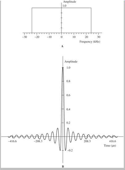
FGR. 8 An impulse response completely characterizes a system. A. The frequency
response of an ideal brick-wall lowpass filter with a 24-kHz cutoff frequency.
B. The time domain impulse response of the ideal brick-wall filter shown above.
The sin(x)/x function passes through 0 at multiples of the sampling period
of 1/48,000 Hz. The ringing thus occurs at 24 kHz.
The action of lowpass filtering, and the impulse response, is summarized in Fgr. 9. In this example, the input signal comprises two sine waves of different frequencies Fgr. 9A); their spectra consist of two lines at the sine wave frequencies ( Fgr. 9B). Suppose that we wish to lowpass filter the signal to remove the higher frequency. This is accomplished by multiplying the input spectra with an ideal lowpass filter characteristic ( Fgr. 9D), producing the single spectral line ( Fgr. 9F). The time-domain impulse response of this ideal lowpass filter follows a sin(x)/x function ( Fgr. 9C); if the input time domain signal is convolved with the sin(x)/x function, the result is the filtered output time-domain signal ( Fgr. 9E). In other words, a time-domain, sampled signal can be filtered by applying the time-domain impulse response that describes the filter's characteristic. In digital systems, both the signal and the impulse response are represented by discrete values; the impulse response of an ideal reconstruction filter is zero at all sample times, except at one central point.
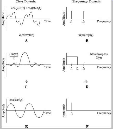
FGR. 9 An example of lowpass filtering shown in the time domain (left column)
and the frequency domain (right column). A. The input signal comprises two
sine waves. B. Spectrum of the input signal. C. Impulse response of the desired
lowpass filter is a sin(x)/x function. D. Desired lowpass filter transfer function.
E. Output filtered signal is the convolution of the input with the impulse
response. F. Spectrum of the output filtered signal is the multiplication of
the input by the transfer function.
An ideal brick-wall output filter reconstructs the audio waveform. Although the idea of smoothing the output samples to remove high frequencies is essentially correct, a more analytical analysis shows exactly how waveform reconstruction is accomplished by lowpass filtering. An ideal brick-wall lowpass filter is needed to exactly reconstruct the output waveform from samples; the sampling theorem dictates this. As noted, an ideal brick wall lowpass filter has a sin(x)/x impulse response. When samples of a bandlimited input signal are processed (convolved) with a sin(x)/x function, the band-limited input signal represented by the samples will be exactly reproduced; the sampling theorem guarantees this.
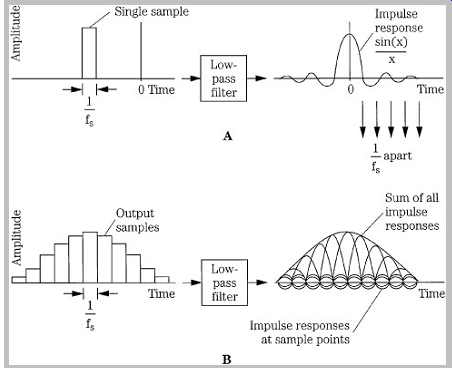
FGR. 10 The impulse response of an ideal lowpass filter reconstructs the
output analog waveform. A. The impulse response of an ideal lowpass filter
is a sin(x)/x function; it’s truncated in this drawing. B. When a series of
impulses (samples) are lowpass-filtered, the individual impulse responses sum
to form the output waveform.
Specifically, as shown in Fgr. 10A, when a single rectangular audio sample passes through an ideal lowpass filter, after a filter delay it emerges with a sin(x)/x response.
If the lowpass filter has a cutoff frequency at the half sampling point (fs/2) then the sin(x)/x curve passes through zero at multiples of 1/fs. When a series of audio samples pass through the filter, the resulting waveform is the delayed summation of all the individual sin(x)/x contributions of the individual samples, as shown in Fig. 10B. Each sample's impulse response is zero at the 1/fs position of any other sample's maximum response. The output waveform has the value of each sample at sample time, and the summed response of the impulse responses of all samples between sample times. This superposition, or summation, of individual impulse responses forms all the intermediate parts of the continuous reconstructed waveform. In other words, when the high-frequency staircase components are removed, the remaining fundamental passes exactly through the same points as the original filtered waveform.
Output filtering, with an ideal lowpass filter, yields an output audio waveform that is theoretically identical to the input bandlimited audio waveform. In other words, it’s the filter's impulse response to the audio samples that reconstructs the original audio waveform. To summarize mathematically, we see that an ideal brick-wall filter outputs a sin(x)/x function at each sample time; moreover, the amplitude of each of these functions corresponds to the amplitude of the sample; when all the sin(x)/x functions are summed, the audio waveform is reconstructed.
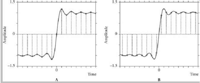
FGR. 11 An audio signal is correctly reconstructed regardless of the sample
location relative to the waveform timing. A. A bandlimited step is sampled
with a sample at a zero-crossing time. B. A bandlimited step is sampled with
samples symmetrical about the zero-crossing time. In these cases, and in other
cases where samples occur at other times, the same waveform is reconstructed.
(Lipshitz and Vanderkooy)
To return to a question posed in Section 2, we can again ask whether samples can capture waveform information that occurs between samples. The impulse response shows that they do. Moreover, the capture is successful no matter where the samples occur in relation to the waveform's timing. Stanley Lipshitz and John Vanderkooy have concisely illustrated this. In Fgr. 11A, a sample happens to fall exactly at the zero-crossing of a step waveform. The bandlimited step waveform (the heavy line) is reproduced (by the summed sin(x)/x functions). In Fgr. 11B, samples fall at either side of the zero-crossing.
Again, the waveform (heavy line) is exactly reconstructed.
Similarly, the same waveform would be reconstructed no matter where the samples lie, and the zero-crossing time is the same. Also, non-intuitively, a higher sampling frequency does not somehow improve the resolution of the successful capture and reconstruction of this bandlimited waveform.
Digital Filters
Because of the phase shift and distortion they introduce, analog brick-wall output filters have been abandoned by manufacturers, in favor of digital filters. A digital filter is a circuit (or algorithm) that accepts audio samples and outputs audio samples; the values of the throughput audio samples are altered to produce filtering. When used on the output of a digital audio system, the digital filter simulates the process of ideal lowpass filtering and thus provides waveform reconstruction. Rather than suppress high frequency images after the signal has been converted to analog form, digital filters perform the same function in the digital domain, prior to D/A conversion. Following D/A conversion, a gentle, low-order analog filter removes remaining images that are present at very high frequencies.
In most cases, finite impulse response (FIR) digital filters are used; oversampling techniques allow a less complex digital filter design. With oversampling, additional sample values are computed by interpolating between original samples. Because additional samples are generated (perhaps two, four, or eight times as many), the sampling frequency of the output signal is greater than the input signal. A transversal filter architecture is typically used; it comprises a series of delays, multipliers, and adders.
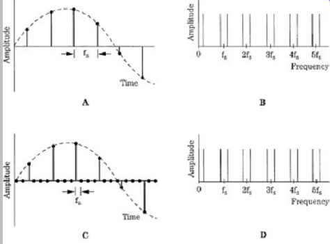
The task of an oversampling filter is twofold: to resample, and to filter through interpolation. The signal input to the filter is sampled at fs, and has images centered around multiples of fs, as shown in Fgrs. 12A and B.
Resampling begins by increasing the sampling frequency.
That is accomplished by injecting zero-valued samples between original samples at some interpolation ratio. For example , for four-times oversampling, three zero-valued samples are inserted for every original sample as shown in Fgr. 12C. The oversampling sampling frequency equals the interpolation ratio times the input sampling frequency, but the spectrum of the oversampled signal is the same as the original signal spectrum, as shown in Fgr. 12D. In this case , for example, with an input sampling frequency of 48 kHz, the oversampling frequency is 192 kHz. This data enters the lowpass digital filter with a cutoff frequency of fs/2, operating at an effective frequency of 192 kHz.
Although the original data was sampled at 48 kHz, with oversampling it’s conceptually indistinguishable from data originally sampled at 192 kHz. The zero-packed signal is passed through a digital lowpass filter with the time-domain impulse response shown in Fgr. 12E. The low-pass filter's frequency-domain transfer function is shown in Fig. 12F. The fixed sample values in Fgr. 12E, occurring at the oversampling frequency, comprise the coefficients of the digital transversal lowpass filter. The input (oversampled) samples convolved with the impulse response coefficients yield the filter's output. In particular, the filter's output is an interpolated digital signal, as shown in Fgr. 12G, with images centered around multiples of the higher oversampling frequency fa, as shown in Fgr. 12H.
To recapitulate, interpolation is used to create the intermediate sample points. In a four-times oversampling filter, the filter outputs four samples for every original sample. However, to be useful, these samples must be computed according to a certain algorithm. Specifically, each intermediate sample is multiplied by the appropriate sin(x)/x coefficient corresponding to its contribution to the overall impulse response of the lowpass filter in the time domain (see Fgr. 10B). The sin(x)/x function in the time domain has zeros exactly aligned with sample times, except at the sample currently being interpolated. Thus, every interpolated sample is a linear combination of all other input samples, weighted by the sin(x)/x function. The multiplication products are summed together to produce the output-filtered sample. The conceptual operation of a digital filter thus corresponds exactly to the summed impulse response operation of an ideal analog brick-wall filter. Spectral images appear at multiples of the oversampled sampling frequency. Because the distance between the baseband and sidebands is larger, a gentle low-order analog filter can remove the images without causing a phase shift or other artifacts.
The oversampling ratio can be defined as:

where fa = the oversampling frequency and fs = the input sampling frequency.
Oversampling initially requires insertion of (R - 1) zero samples per input sample. The samples created by oversampling must be placed symmetrically between the input samples. A lowpass filter is used to bandlimit the input data to fs/2, with spectral images at integer multiples of (R × fs). Moreover, lowpass filtering creates the intermediate sample values through interpolation. Rather than perform multiplication on zero samples, redundancy can be used advantageously to design a more efficient filter.
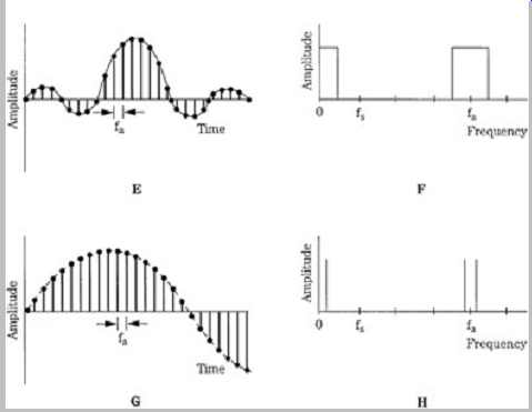
FGR. 12 An oversampling filter resamples and interpolates the signal, using
the impulse response; this is shown in the time domain (left column) and frequency
domain (right column). A. The input signal is sampled at fs. B. The signal
spectrum has images centered around multiples of fs. C. With resampling, zero-valued
samples are placed between original samples at some interpolation ratio. D.
The spectrum of the oversampled signal is the same as the original signal spectrum.
E. The values of a sampled impulse response correspond to the coefficients
of the digital filter. F. The transfer function of the filter shows passbands
in the audio band and oversampling band. G. The digital filter performs interpolation
to form new output sample values. H. The output-filtered signal has images
centered around multiples of the oversampling frequency, fa.
FIR Oversampling Filter
As we have seen, a digital filter can use an impulse response as the basis of the computation to filter the audio signal. When the impulse response uses a finite number of points, the filter is called a finite impulse response (FIR) filter. In addition, in the case of an output lowpass filter, oversampling is used to extend the Nyquist frequency.
Fgr. 13 shows a four-times oversampling FIR digital filter, generating three intermediate samples between each input sample. The filter consists of a shift register of 24 delay elements, each delaying a 16-bit sample for one input sampling period. Thus each sample remains in each delay element for a sample period before it shifts to the next delay element. During this time each 16-bit sample is tapped off the delay line and multiplied four times by a 12 bit coefficient stored in ROM, a different coefficient for each multiplication, with different coefficients for each tap. In total, the four sets of coefficients are applied to the samples in turn, thus producing four output values. The 24 multiplication products are summed four times during each period, and are output from the filter. The filter characteristic (sin(x)/x in this case) determines the values of the interpolated samples. Each 16-bit data word is passed to the next delay (traversing the entire delay line), where the process is repeated. Many samples are simultaneously present in the delay line, and the computed impulse responses of these many samples are summed.
The product of each multiplication is a 28-bit word (16 + 12 = 28). When these products are summed, a weighted average of a large number of samples is obtained. Four times as many samples are present after oversampling, with interpolation values calculated by the filter. In this example, the sampling frequency is increased four times, to 192 kHz. The result is the multiplication of the sampling frequency, and a cutoff filter characteristic. Through proper selection of filter coefficients, length of delay line, and time interval between taps, the desired lowpass sin(x)/x response is obtained-yielding correct waveform reconstruction. Because of the movement of the data across the shift register, this design is often called a transversal filter.
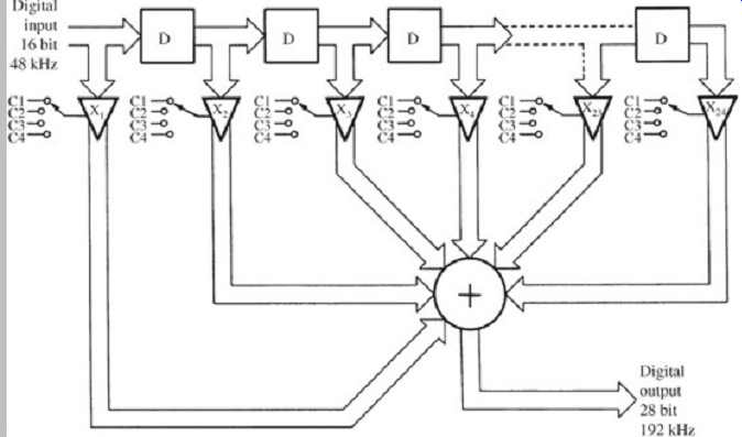
FGR. 13 Twenty-four element digital transversal filter showing a tapped delay
line, coefficient multipliers, and an adder.
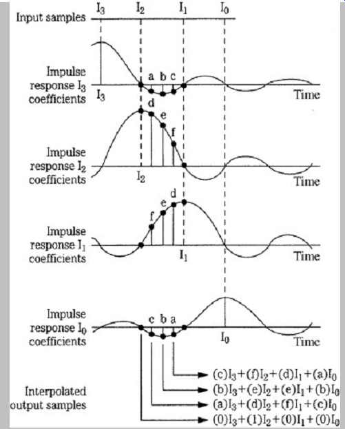
FGR. 14 A four-times oversampling filter treats input samples as points on
a sin(x)/x curve; this reconstructs the output waveform, as in an ideal lowpass
filter. In practice, many more samples are needed.
Fgr. 14 illustrates how an oversampling digital filter simulates the effect of an analog filter in waveform reconstruction; specifically, it shows how interpolated samples are computed in a four-times oversampling filter.
The input samples I3, I2, I1, and I0 are treated as sin(x)/x impulses placed relative to the center of the filter. Their maximum sin(x)/x impulse response amplitudes are equal to the original sample amplitudes, and the width of the impulse responses are determined by the response of the filter, in this case a filter with a cutoff frequency at the Nyquist frequency of the input samples. The summation of their unique contributions forms the interpolated samples (in practice, as noted, many more than four samples would be present in the filter). Each of the three interpolated samples is formed by adding together the four products, as shown in the figure. Original input samples pass through the filter unchanged by using one set of filter coefficients that contains three zero coefficients and one unity coefficient. In this way, the output sample that coincides with the input sample is unchanged. By multiplying each group of samples (four in this case) with this coefficient set, and three others, interpolated samples are output at a four times rate.
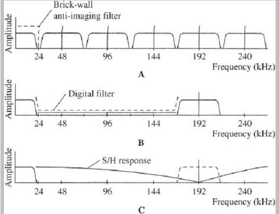
FGR. 15 Image spectra in nonoversampled and oversampled reconstructions.
A. A brick-wall filter must sharply bandlimit the output spectra. B. With four-times
oversampling, images appear only at the oversampling frequency. C. The output
S/H circuit can be used to further suppress the oversampling spectra.
The overall effect of four-times oversampling filtering is shown in Fgr. 15. A brick-wall filter must sharply bandlimit the output spectra; with oversampling filtering, the images between 24 kHz and 168 kHz (centered at 48, 96, and 144 kHz) are suppressed, leaving the oversampling images.
The output S/H circuit can be used to further suppress the oversampling spectra, as shown. In practice, a number of considerations determine the design of oversampling filters. The sin(x)/x waveform extends to infinity in both the positive and negative directions, so theoretically all the values of that infinite waveform would be required to reconstruct the analog signal. Although an analog filter can theoretically access an infinite number of samples for each reconstruction value, a finite impulse response filter, as its name implies, cannot. Thus the oversampling filter is designed to accommodate the number of samples required to maintain an error less than the system's overall resolution. In the example above, only four coefficients were used, but as many as 300 28-bit coefficients might be needed; in practice, perhaps 100 coefficients would suffice. However, because the sin(x)/x response is symmetrical, only half the coefficients need to be stored in memory; the table can be read bidirectionally. As noted, the multipliers in a digital filter increase the output word length.
The output word cannot simply be truncated; this would increase distortion. The word should be redithered.
These examples have used a four-times oversampling filter. However, two-times, four-times, or (most commonly) eight-times digital filters can be used, in which a 48-kHz sampling frequency is oversampled to 96, 192, or 384 kHz, respectively. For example, in an eight-times oversampling filter, seven new audio samples are computed for each input sample, raising the output sampling frequency to 384 kHz. Images are shifted to a band centered at 384 kHz where they are easily removed with a simple analog lowpass filter. Whatever the rate, most oversampling digital filters are similar in operation. However, the characteristic of the analog lowpass filter varies. The lower the oversampling frequency, the closer to the audio band the image spectrum will be, hence the steeper the analog filter response required.
When using traditional D/A converters, a practical limit to the oversampling frequency is reached (around eight times) because most D/A converters cannot operate at faster speeds. On the other hand, D/A converters can more easily convert an oversampling waveform, because the successive changes in amplitude are smaller in an over sampled signal. More precisely, the slew rate, the rate of variation in the output waveform, is lower. This, along with less ringing and less overshoot, reduces intermodulation distortion. Some designers feel that in oversampling designs of eight times or more, the remaining image spectrum is at such a high frequency that analog filtering can be accomplished with a simple second-order lowpass filter.
In terms of performance, digital filters represent a great improvement over analog filters because a digital filter can be designed with considerable and stable precision.
Because digital filtering is a purely numerical process, the characteristics of digital filtering, as opposed to analog filtering, cannot change with temperature, age, and so on. A digital filter might provide an in-band ripple of ±0.00001 dB, with a stopband attenuation of -120 dB. A digital filter can have a linear phase response. High-frequency attenuation due to aperture error can be compensated for in the transversal filter by choosing coefficients to create a slightly rising characteristic prior to cutoff. Digital filter theory is discussed in Section 17.
(cont. >>)
