Low-voltage power supplies used to be, in the days of simple vacuum tubes, just a matter of whether you had a "hot" or "cold" chassis and, perhaps, whether rectifiers were either half-wave or full-wave. In the less expensive receivers, this outlook hasn't changed much, because of the lower cost involved. But in the better color sets, there's now a considerable choice with many, many engineering advances in the past two years and, apparently, considerably more to come. For in stance, the industry is talking right now about switched power supplies for everything but the collector voltage of the horizontal oscillator, and this could be the only directly rectified feed. All other voltages could come from power circuits that would be driven, probably, by the horizontal oscillator, or higher or lower frequencies thereof. A big advantage would be better short circuit protection, which is very important with semiconductors. Others include much less filtering at the higher frequencies, a completely modularized power supply, less costly low-voltage transformers, and reduced ripple on the bus feeders, to name a few. Motorola, in fact, is already doing just this, and has additional ideas in the engineering think tank for the future. RCA, also has a partially plug-in power supply, with regulators among the modules, and the removal of modules in certain Zenith receivers will disable DC immediately.
Romancing power supplies has been a pretty dull job until recently, but the already tremendous setup and competition in consumer products will certainly result in many unique and useful innovations now and in the years ahead. And it may just come to pass that the active filter principle, used in the past several years by Sylvania, may be well worth adding to the very advantageous oscillator switching method of developing power.
POWER SUPPLY BLOCK DIAGRAM
The block diagram in Fig. 11-1A is typical of the power supply found in better receivers. AC passes through the line cord into the receiver interlock and coil line filters, then through the voltage-dependent resistor that, when cold, exhibits little resistance. In a second or two, the screen area is degaussed, but no substantial AC reaches the isolating stepup or stepdown transformer. In a moment, however, the thermistor gets hot, decreases quickly in resistance, and current passes directly to the transformer primary while the VDR blocks all AC from the degaussing coils. The transformer secondary supplies the rectifiers, which usually pass the positive alternations and block the negative ones. The resulting DC ripple is now filtered by chokes, resistors, and capacitors and passed, non-regulated, to circuits like the audio output, CRT, etc. The more critical portions of the receiver, such as transistorized IFs, video amplifiers, and the chroma circuits-especially if these are semiconductors-receive regulated supply voltages.
In the less expensive version in Fig. 11-1B, we didn't bother to put in a degaussing coil, since it would be the same principle, but we do show a half-wave voltage doubler, with one side of the AC line connected directly to receiver chassis.
This is the "touchier" type power supply where-if the AC plug has the right (or the wrong!) polarity and you have your hand on ground or a cold water pipe-you could become an instant angel with no difficulty. ALWAYS use an isolation transformer when you're working with one of these, not only to protect yourself but your test equipment, too. Well-regulated changes of 20 or 30 amperes and 115 to 120-volts (some 2300 to 3600 volt-amperes) play few favorites. Most unfortunates never live to recognize their mistake.
In case you meet this voltage doubler in your work, here's how it works: On the negative alternation, C1 charges through D1 to 150 volts. On the positive alternation, C1 discharges through D2, charging C3 and C4 by way of L1 (for C4). The 120-volt input, naturally, is doubled through a 150-mfd capacitor, and comes to D2 at about 300 volts. Then there's a 20- to 40-volt drop because of rectification loads, and dividers. The capacitors are low impedances to AC ripple, while the choke is a low-impedance to DC and a high impedance to AC. The ripple frequency, in this instance, is 60 Hz, always a tough one to filter, while ripple in the supply diagrammed in Fig. 11-1A is 120 Hz, since you'd have full-wave or bridge rectification. The faster the frequency the less and more uniform the ripple and the easier it is to smooth out by filters, where component values decrease somewhat in proportion to frequency.
Remember;
C = ½ pi fXc
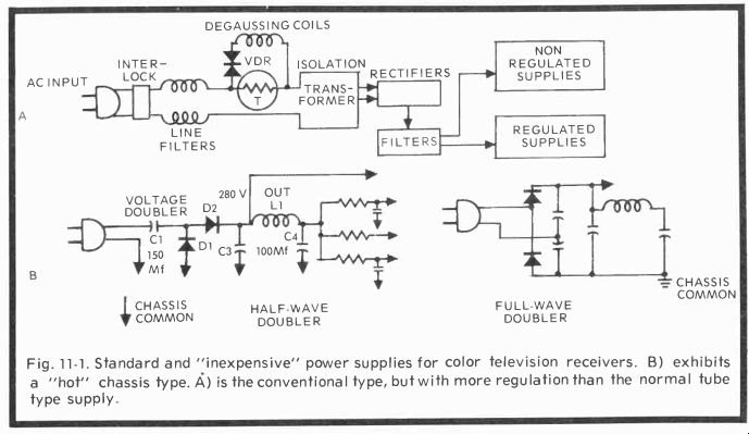
Fig. 11-1. Standard and "inexpensive" power supplies for color
television receivers. B) exhibits a "hot" chassis type. A) is the
conventional type, but with more regulation than the normal tube type supply.
You might also recall that RMS is the equivalent sine-wave energy for DC power; then RMS X 1.414 equals peak, and RMS X 1.414 X 2 equals peak-to-peak.
SEMICONDUCTOR BRIDGE POWER SUPPLY FOR VACUUM TUBES
Since solid-state diodes generate much less heat, are relatively reliable, and maintain their efficiency to the point of life expiration, the more recent color receiver tube power supplies employ this type of rectifier. Also, a bridge rectifier is more effective and with it, a smaller power transformer can be used instead of the very heavy type associated with the usual full-wave diode or tube supply.
In Fig. 11-2, we have a diode bridge rectifier that receives AC from the secondary of the power transformer after current has passed through RF chokes L115A and B and the associated RC filter networks on either side of the input line. Normal voltage input goes to the BLK-RED tap. In high line-voltage situations, the BLK-WHT tap is used.
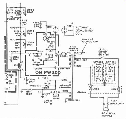
Fig. 11-2. Standard unregulated bridge-type supply circuit for vacuum tube
receivers.
Current passes initially through the degaussing coil until thermistor RT201 heats and shunts AC directly to SR201. On a positive alternation at the top of the transformer winding SR201 conducts, SR202 and SR203 are back biased, and the capacitors in the voltage divider string and on the other side of choke L107 charge. Current returns to the lower half of the transformer secondary through ground and SR204. When the lower (GRN-RED) half of the transformer is positive, SR203 conducts, SR201 and SR204 are back biased, and the current return to the upper half of the transformer is through ground and SR202. All capacitors are fully charged after several alternations, degaussing, of course, is cut off, and the receiver "sees" all voltages, including the +420 volts of virtually un filtered supply that furnishes DC potential for the cathode ray tube filaments. The 420-volt supply keeps the CRT cathode heater potential close enough to prevent serious arcs and consequent damage to the tube.
In troubleshooting such a supply, first measure the various voltages, then look at the AC ripple wherever a voltage is down. When a capacitor fails to charge, is leaky, or shorted to ground, you'll have a lower voltage or no voltage at all. In the first instance, there will be high ripple-probably 10 or more volts. In the second case, obviously, you'll measure nothing or almost nothing, and the capacitor will have to be disconnected to prove its condition. However, when a capacitor shorts, it usually draws current through a resistor which burns, or at least smokes. Don't just replace the resistor and pray; measure resistance along the line where the burned resistor is connected and discover why. And do not use an ohmmeter to measure capacitance, either for opens or leak age; it simply can't be done. Use a capacitance checker or a current meter, but never an ohmmeter! An oscilloscope with an LC probe will show you any measurement of AC ripple. And any excessive ripple can always be identified by shunting a filter capacitor across the line to ground. If the ripple sub sides, you can go find the bad capacitor. If it doesn't, check the frequency of the ripple and find out what section of the receiver is radiating. Then find your bad filter and fix it! When-and this applies strongly to semiconductor power supplies-you have lowered voltages along one or more power feeder lines, disconnect each line, one by one, until the load returns to normal. This identifies the problem circuit. Next, you have to find the stage, and then the cause of the trouble in that stage.
In power supply troubleshooting, the method you use is king. These solid-state receivers cannot be shot-gunned. If you don't believe me, try it. Your shop will pay a big bill to have your work done over, and you may not have a job. We deliberately discussed troubleshooting here to make you very aware of the basic methods for handling troubles in power supplies. In some of the more sophisticated DC sources we'll be talking about, you'll have to go far beyond the basics to handle their special problems efficiently. The "disconnect" procedure, however, is always a successful technique in any complex that is either a high supplier or high user of current and never forget that a transistor is a current-operated device with DC biasing its most sensitive and demanding parameter.
The reason is that a bipolar semiconductor is substantially a low-impedance device, while a vacuum tube, and its semiconductor cousin, the FET, are voltage-operate high-impedance devices, at least input-wise.
It is worth remembering that in a bipolar: Ie (emitter current) equals Ic (collector current) + lb (base current) and that the static current gain equations for the three transistor configurations are:
Ic h =-fb le Ic "fe IT Ie hfc = I b common base common emitter common collector while the common-base current gain is:
- Beta Al pha Beta + 1 common emitter current gain is:
Therefore, Ic equals BIb, or in the full expression:
Ic = BIb + (B + 1) (Icbo) taking into account the leakage from collector to base with the emitter open. In a vacuum tube, amplification factor (mu) equals transconductance (gm) x plate resistance (rp) ; so:
In a field-effect transistor; gm equals Id (drain current) divided by Vgs (voltage, gate-to-source) and Av (voltage gain) equals gm x ZL.
In all this, you can begin to see the similarity between FETs and tubes, except the FET, and especially the MOSFET, a metal oxide semiconductor, are even more useful devices than the vacuum tube. They can do more things, with great bandpass and speed, and still don't need the huge voltages and currents most vacuum tubes must have.
ZENITH'S 25CC55 REGULATED SOLID-STATE SUPPLY
This 25CC55 power supply offers a separate winding on the secondary for the degaussing coils, extra filtering in the regulator portion, and a new limit switch. The limit switch is interesting in that high-voltage pulses from the flyback are rectified by CR210, then filtered by C242. The remaining DC, when it becomes large enough, fires the 3AGB PL1 lamp, and this causes Q209 to conduct to ground, shutting off the regulated 24-volt supply for as long as PL1 is lighted. This now makes the receiver comply with FCC regulations. Otherwise, under normal operation, Q209 is not in conduction.
With Q209 off and Q212 producing normal regulation, R324 can be considered the load resistor. R326 is the source-to-base bias, load and limiter for reference zener CR213. C241 is a filter. Changes in the load or collector voltage are referenced to CR213 and the transistor corrects its voltage output accordingly. The protection resistor is 20-watt R322, which will take most of the current if there is a short through either Q212 or Q209, with F203 as a final fuse backup in case of extraordinary overload.
The voltage-sensing circuit also has a bit of a turn-around compared with earlier supplies, with B+ adjust in the emitter of Q214, a thermistor between emitter and base, zener reference in the base, and a 250-volt voltage input bus that is rectified and filtered from a source in the primary of the flyback transformer. CR222 through CR225, the main bridge rectifiers, do exactly what the previous bridge did, this time with CR223 and CR224 conducting first, then CR225 and CR222.
Return by way of ground passes through interlocks on the chroma, 3.58-MHz subcarrier, AGC, and vertical modules, so that any break in this continuity shuts off DC for the entire power supply. The horizontal oscillator is on another DC hot line at the output of the bridge, and a defect in those circuits will cut off the voltage driver, regulator, etc.
Voltage developed at the output of the bridge is 160 volts, which is filtered to supply the audio stages and the voltage driver and regulator transistors. As is shown in Fig. 11-4, the side pincushion correction circuit is a vital part of the regulated power supply. A 60-Hz parabolic waveform is supplied by the vertical output transformer, but with a large positive spike that is blocked at the base of Q211 by CR212. The pure parabolic voltage is now amplified and inverted by Q211 and is AC coupled to the base of voltage sensor Q214 (Fig. 11 3). This transistor's base reference is zener diode CR215, with bias supplied from both emitter and collector by a network of resistors that also supply a DC component from the flyback 250-volt source. The DC output is set by R338, the B+ adjust.
This feeds the base of Q213, which, through its emitter, sup plies the base of regulator Q215.
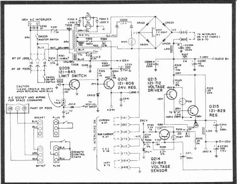
Fig. 11-3. Revised power supply appearing in Zenith's all solid-state 25CC55
receivers. PL1 lamp stays lit with overvoltage HV surge until the receiver
is turned off, then on. PL1 when on kills the +24-volt supply.
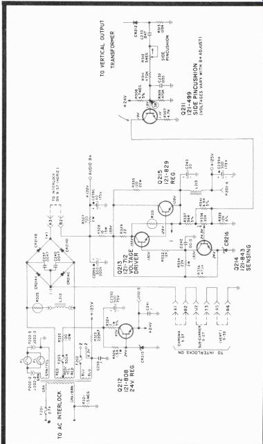
Fig. 11-4. The original low-voltage supply circuit for the 40BC50 Zenith
and side pincushion correction circuit.
Since the reference diode has a fixed voltage (in one case, 140 volts and in the other 24-volts), any change in voltage will result in a change of current through Q214, reducing or raising the bias on Q213, and so regulating the output of Q215. Below the AC protection varistor, you will see an arrow to the horizontal output transformer and you will also observe the side pincushion amplifier bus coming into the circuit between R337 and R338. What happens here is that the vertical 60-Hz parabola actually modulates the B+ to the horizontal output transformer and expands the B+ with vertical scan to change the picture width to compensate for pincushion distortion by pushing out the sides of the picture through its middle at a 60-Hz rate. Filtering for the resulting 60-Hz induced ripple is taken care of by R327, C239C, and L213, and C239A and B.
RCA'S CTC46 SUPPLY
The generally sophisticated circuit in Fig. 11-5 has the usual interference reject coils, circuit-breaker and LC filters, high-low line switch, and isolation line transformer with five voltage sources that are all rather carefully filtered and rectified. The individual video and chroma plug-in modules have their separate or collective regulators, instead of single source regulation from the power supply. Both diode bridges work as all bridges do, and there is a thermistor at terminals 4 and 5 to block and shunt current when cold and hot, respectively. After degaussing has been completed, the half-wave CR1 is allowed full current and the 225-volt source comes on to provide drive for the set. A centertap off the 77-volt supply produces the 26- and 30-volt sources for the sound and other circuits.
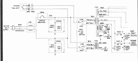
Fig. 11-5. RCA's CTC46 supply. Voltage regulators are on various module plug
boards.
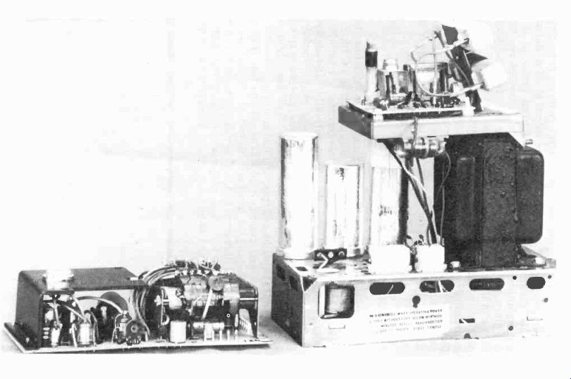
Fig. 11-6. Comparison between Motorola's new switched plug-board power supply
and much larger AC-regulated unit used in the Original Quasars. (Courtesy
Ralph Jones)
One of the handy features of this supply, however, is the plug board (part of PW600) that contains all rectifiers and the large thermistor for the degaussing coil. If you suspect any of these elements being faulty, simply pull the MAB module, substitute another, and find out.
MOTOROLA'S SWITCHING POWER SUPPLY FOR CTV7-8 CHASSIS
Like the "offshore" beginning of Instamatic, Accu-Matic, or by whatever name present chroma and other controls have become known, this general power supply had some foreign origins, too, but its U.S. introduction is very likely the beginning of an era of all sorts of switching power supplies.
Why? Because of utility, less expense, lighter power trans formers, stepdown instead of stepup voltages, and the other advantages named earlier in this section. To this Motorola power supply they all apply. And, since a picture can sometimes tell more than 1,000 words, look at the difference in Fig. 11-6 between Motorola's new and original all-AC regulated Quasar power supplies in terms of filtering, size of components such as capacitors, the power transformer, huge dropping resistors on top the regulator subchassis. In addition, almost the complete supply is made of plug-in modules and can be removed by simply unplugging panel JA in any of the Quasar CTV7 and CTV8 solid-state receivers.
The schematic for the switch mode supply is shown in Fig. 11-7. As you can see, except for full-wave rectifier diodes, filament transformer, several other coils, and the degaussing units, most of the circuitry fits snugly on plug panel JA.
The input voltage doubler is made up of D800, D801, and capacitors C800 and C801, collectively, that are attached to one side of the AC line. C800 also goes to isolated ground. Rectified AC charges C800A, C801 alternately plus the other capacitors, and D800 passes a total WVDC about 300 volts that, because of drops and loads, becomes 280 usable volts. This filtered DC is now brought over the top of panel JA, in through terminal 10, to the primary of low-voltage transformer T3. (In block diagram form, this DC connection and the ensuing circuit description is shown in Fig. 11-8. You may follow both the schematic and block outline together.) DC energizes the primary of the transformer through the action of output switch Q8 to isolated ground. This switch is driven through a series of three other transistors plus a regulator, and all are protected by a silicon controlled rectifier (SCR) crowbar microsecond shut off.
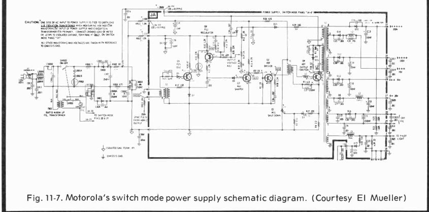
Fig. 11-7. Motorola's switch mode power supply schematic diagram. (Courtesy
El Mueller)
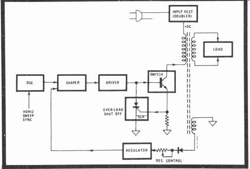
Fig. 11-8. Complete block diagram of the electronic power supply. (Courtesy
Chuck Preston)
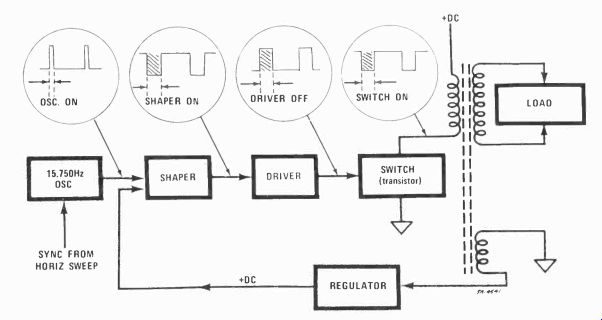
Fig. 11-9. Switched power supply operational diagram with rectangular waveforms.
(Courtesy Stan King).
A 200-volt sync pulse from the 15,734 Hz horizontal output appears across the primary of T2, a blocking oscillator, connected between collector and base of Q5. Thus, the oscillator is synchronized with the receiver's horizontal oscillator and its output is shaped as a rectangular wave to control the driver and, finally, the output switching transistor.
The action is further shown in Fig. 11-9, along with the various waveforms that may be expected. These waveforms are, of course, exhibited for normal conditions only when regulation is unnecessary. But when, say, brightness is increased and the secondary of the transformer needs more power, the Q8 DC switch is closed for a longer time period and primary current increases, thereby satisfying the secondary demand.
The switching transistor is controlled as follows:
Regulator Q4 takes samples of the driven oscillator voltage from a separate winding (pins 3 and 12) on T3, which is routed back to the base of the regulator through diode D15. At the same time, positive DC from the 33-volt bus, regulated by zener D4, and filtered by 50-mfd C18, is the reference DC for the base and emitter of Q4. Another reference is series RC circuit C24 and R35, which is connected between the Q4 base and the 280-volt line, establishing a positive-to-negative charge on the capacitor that can vary with DC voltage changes. Further RC time constants C12, R30, R16, etc., help shape this feedback voltage in the Q4 base-emitter circuit. Any changes in the DC supply will produce an RC change at the base of Q4, resulting in a steepening or lengthening of the sawtooth at the emitter of the regulator, changing the width of the oscillator output waveform and so shaping the final drive pulse to the output switching transistor.
Under extra load conditions, the output switch is kept on longer, therefore, supplying more current to both the primary and secondary of the transformer so that the response promptly fulfills further current drain requirements. Conversely, less supply needs cause the regulator to conduct for shorter periods and so narrows the rectangular drive waveforms for the output switch, keeping it on for a shorter period and so reducing current in the supply.
Pretty much the same situation occurs if the line voltage increases or decreases, and so the supply is regulated both from within and without, and any internal supply transients on the various buses will appear stationary at a 63.5-microsecond time rate. Should the voltage through the output switch reach a level that causes D3 to zener and pass a signal, this will turn on SCR Q1 and the entire supply will shut down until the receiver is turned off (or the circuitbreaker blows) and the anode of the SCR has the voltage removed entirely. Gate voltage turn on will never turn off an SCR, only the removal of its anode potential.
DELCO'S FLYBACK SWITCHING REGULATOR
To show that other companies besides Motorola are already actively thinking about a switched power supply, consider the following material, developed by W.A. Robinson of Delco Electronics. Instead of a blocking oscillator, however, a self-generated Colpitts (two capacitors) oscillator (Q1) is used to produce a sine wave. The Q1 and Q2 emitters and the collector of Q3 are regulated by zener diode D5.
Feedback modulation voltage comes from winding "LT" directly into the emitter of Q2. The feedback voltage and the sine wave are mixed between R13 and R14. This feedback is proportional to the DC output voltage. There is also a feedback effect through R2 in terms of supply voltage, and R2 is also the starting drop resistor for the Colpitts oscillator. Voltage adjustment R11 is located between R10 and R12. R13 actually determines the maximum pulse width, which goes to Q3 (a shaper), to change the sine wave into a pulse of varying width, depending on the feedback and DC reference modulation.
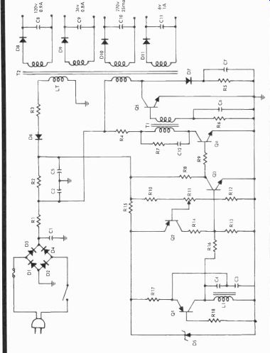
Fig. 11-10. Delco's flyback switching regulator circuit for large screen
color receivers.
Thereafter, driver Q4 supplies energy for the primary of T1, which is flux coupled to the base of switch transistor Q5, the primary switching source for T2. Components R5, D7, and C7, a voltage clamp for Q5, absorb the higher than normal voltage spikes.
Diodes D8 through D11 supply the complete current and operating voltage outputs as shown on the schematic ; 120 volts at 900 milliamperes, 36 volts at 800 milliamperes, 270 volts at 25 milliamperes and 6 volts at 1 ampere. The entire circuit operates at 20 kHz with small T1 and T2 transformers; the first is a laminated steel core type and the second has a ferrite core.
QUESTIONS
1. What is a "cold" chassis, and why do the less expensive receivers have one side of the chassis connected to the AC line?
2. How does C1 in Fig. 11-1B charge on the negative current alternation?
3. A sine-wave peak-to-peak voltage of 340 volts equals what value at RMS?
4. Why are so many 4-bridge diodes used in modern power supplies?
5. What happens when a degaussing thermistor gets hot?
6. When a capacitor in a low-voltage supply opens, what problems occur?
7. Why do you always use an ohmmeter to measure coils and capacitance?
8. The collector current is the sum of the and currents?
9. Show that transconductance equations for FETs and tubes are somewhat similar.
10. Why do you suppose Zenith added a diode-transistor limit switch in the power supply?
11. How does Zenith take care of its solid-state pincushion problem?
12. RCA differs in its power supply philosophy from other set manufacturers. How?
13. Is Motorola's new power supply DC or AC governed in it's regulation function?
14. How do the Delco and Motorola regulators basically differ?
Next: Link | --Chroma Circuits
Also see:
TV Antennas and Transmission lines
Air Time--An Intro to Television Broadcasting
TV and Radio Tube Troubles (1958)