In the past, vertical oscillator circuits have run the gamut from blocking oscillators, single-tube and common-cathode coupled multivibrators to circuits where the oscillator and output functions both were performed by a dual-purpose tube.
Until the advent of solid state, an output transformer coupled the sweep signal to the yoke. Transistorized circuits use capacitor coupling directly to the deflection yoke. To top it off, there are now thick film vertical modules, and even an all-integrated circuit oscillator and output combination in a plastic package mounted on a heat sink.
The FCC vertical deflection specifications continue to remain the same, however. Each field must be scanned in 1/59.94 Hz, two fields to a frame, with 30 frames produced each second. The field scan time is 16.664 milliseconds, and the blanking interval, included in this count, is 1.4 milliseconds the interval where broadcast sync and equalizing signals are inserted so they will not interfere with color and monochrome video.
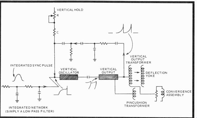
Fig. 8-1. Block diagram of a conventional vertical oscillator output color
subsystem.
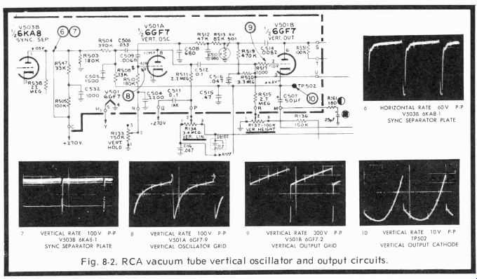
Fig. 8-2. RCA vacuum tube vertical oscillator and output circuits.
Since vertical circuits operate quite close to house current frequency, they're not hard to build, but to design them with excellent linearity sans all sorts of control interaction is, to put it mildly, somewhat more than difficult. But we should see an end to such problems with thick film and even monolithic ICs where current generators are more commonplace. General Electric already has a monochrome receiver where separation has already been designed in at routine cost, ac cording to engineer John Jordan.
VERTICAL OSCILLATOR-OUTPUT BLOCK DIAGRAM
As an example, let's consider a conventional (tube or transistor) vertical subsystem (Fig. 8-1) with the usual low pass filter integrator network which blocks horizontal sync and shapes the vertical sync pulse. Vertical sync reaches the oscillator either in negative or positive polarity, depending on the circuit, to narrow or increase the conduction period of the oscillator and, consequently, either speed it up or slow it down.
Tube-type oscillators deliver a trapezoidal waveform (a combination of pulse and sawtooth voltage) and transistor oscillators produce a simple sawtooth pulse. Usually, the output is cut off for the duration of the vertical blanking period denoted especially by the high overshoot portion of the vertical output waveform. From the output a portion of the cutoff voltage is fed back to the input of the vertical oscillator, developing an exponential type of voltage shown immediately after the integrated sync pulse, but not necessarily in proportion. When there is no incoming sync, R and C form a time constant that keeps the oscillator-output combination in flywheel operation so that a raster remains on the screen.
The vertical output supplies the vertical output trans former, and pincushion transformer.
Vacuum Tube Sweep System
Fig. 8-2 is typical of the vacuum tube circuits found in the remaining non-semiconductor receivers today. And even though the particular receiver we're discussing is a 1967 model, many other tube sets have duplicated much of the circuit because it's both simple and relatively reliable. Notice the 285-volt (and higher) plate voltages, the multitude of capacitors, and all the half-watt and larger resistors that mush be added to develop the waveforms and time constants that make a vertical oscillator (V501A) and output (V501B) work together for a 1200 to 1500-volt output waveform. Com pare this plethora of components and the operating potentials with those in the modular transistor and integrated circuits to follow ! In Fig. 8-2, sync from V503B (point 6) is applied to an integrating network (point 7) consisting of R504, C505 and C506 to the plate of the vertical oscillator and grid of the vertical output. Such a sync pulse could be strong enough to modify plate operation of the vertical oscillator, but especially the grid of the vertical output, since it is negative-going and can delay or speed up conduction of the output to time the receiver's oscillator. R508 is a voltage divider, while C504, C509, R510, and R133 form a filter and time constant network from the vertical output plate feedback which keeps the oscillator fly-wheeling at an approximate 59.95-Hz rate when there are no incoming sync pulses.
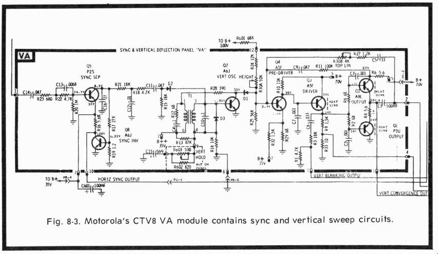
Fig. 8-3. Motorola's CTV8 VA module contains sync and vertical sweep circuits.
Vertical linearity control R134 varies the oscillator plate voltage which is drawn from the 1150 boosted-boost supply in the high voltage. C511, R511, C512 and the voltage variation determine the linearity of the vertical trace during forward conduction. R520 and C516 are the main pulse-shaping components for the vertical output grid, to which is connected the DC height control from the 405-volt supply that determines the DC drive on the grid of the vertical output. C515 is simply a filter to pick up any transients from the suppressor grid of the horizontal output tube where the adjacent downward lead goes. Thereafter, 50-mfd filter C507 couples a 10-volt parabolic pulse from the vertical output cathode to the vertical section of the dynamic convergence assembly. The pulse is filtered by R161 and the 25-mfd capacitor.
The oscillator feedback network begins in the plate circuit of the vertical output. Feedback flows through C514 (DC blocking), a varistor (an AC sensitive resistor; when AC increases, resistance decreases), voltage divider R512-513, C508 and C510-integrating-type capacitors that shape the pulse so that it appears as shown in waveform 8. The waveform's sharp drop occurs when the tube drives suddenly into conduction, then the capacitors take over and permit an exponential curve until the oscillator cuts off, generating a small spike just prior to steep negative-going conduction. This tube does complete a full cycle swing since its DC plate is 285 volts and the peak-to peak voltage shown at the grid of the output tube is 300v. The grid waveform, on the other hand, measures only 100 volts.
Here's an interesting point about that AC grid voltage:
The exponential part of the capacitor discharge time goes up to DC (or zero) and only the spike goes positive enough to drive the oscillator tube into full conduction. The output stage drives the vertical output transformer, a pincushion correction transformer and vertical deflection yoke. In vacuum tube receivers, the inductive kick from the output transformer as the output stage turns off is several hundred extra volts-a good reason for RV501.
Motorola Modular Vertical Circuit
In Motorola's transistorized vertical circuit in the CTV8 series (Fig. 8-4), sync is coupled through C14 and the associated components to the base of the sync separator from the sync output stage in the collector of the second video amplifier. The emitter signal is swamped (filtered) by 100 mfd capacitor C601, but the collector signal is split two ways:
Voltage divider R17 and R19 provide bias for the Q8 sync inverter which reverses the phase of the horizontal sync pulse so that it will turn on the color gate pulse former on the adjacent panel (not shown) and also sync the horizontal oscillator. R15, R18, and R21, plus C11 and C12, form the capacitor charge-discharge integrating network for the vertical oscillator. While D2 is a guide and blocking diode that permits forward positive pulses but blocks negative ones. The blocking oscillator and its RC timing circuits are between the collector and base of vertical oscillator transistor Q7. As usual, the vertical hold is very much a bias circuit; C15 is part of the RC time constant with R603, and D3 is a limiting diode that will conduct and clamp when negative voltage swings produce sufficient negative bias. The height control is pretty much a voltage adjust for the collector of Q7 through guide diode D1 and, since it's purely resistive, the height should be quite linear. Top linearity control R308 is in the feedback loop between output terminal 2 and the base of pre-driver Q4 and is a series voltage adjust.
The primary and secondary of T1 are shunted by C4 and C10 so that the transformer is approximately resonant at 59.94 Hz. The frequency can be adjusted by varying the DC through the coil with the hold control and by the incoming frequency of the positive-going vertical sync pulse. Capacitors C4, C10 and C15 charge during the oscillator cutoff time through the B++ at terminal 7, and discharge rapidly through Q7 and perhaps R14. A blocking oscillator is used because of the better frequency stability over a wider temperature range; they're now small and less expensive, and greater linearity is possible with fewer external components.
When power is first applied, C4, C10 and C15, charge rapidly through the applied DC voltage until they reach a value that is positive enough for the oscillator to conduct.
Since Q7 is simply a transistor switch, its cycle shorts to ground, discharging the capacitors and, in so doing, drops the forward base voltage enough to cut itself off. The capacitors then charge all over again, bring the base to the conduction level, once more biasing the vertical oscillator into conduction. The DC divider action of R603, along with incremental discharges of C15, set the timing for the oscillator.
As Q7 becomes a 16.664-millisecond switch, it causes conduction in the emitter forward biased pre-driver (an inverter) that turns on the driver. The driver, via an emitter connection, supplies vertical blanking, positive vertical pulses for the convergence panel (not shown), and switching for the complementary vertical output. Since Q2 is an NPN type and Q1 a PNP type, the negative and positive gating from the driver turns on first one and then the other for a low-impedance push-pull output that is used for both vertical convergence and to drive the vertical deflection coils with a linear sawtooth deflection current. Capacitors C2 and C3, shunting each transistor base-to-collector, are low-pass filters called wave-shapers and transient suppressors. The output reactance of C1 (500 mfd), by the way, is 5.33 ohms at 59.94 Hz, a rather low impedance.
Troubleshooting some of these DC-coupled stages can be quite another matter, as an illustrative analysis will indicate.
Suppose, for instance, the vertical oscillator quit for some reason and the height control was turned to a midpoint value of 25K. The voltage at the base of pre-driver Q4 would become 39 volts, driving this transistor into saturation; its collector voltage would drop well below the 34 volts at the emitter of Q3, cutting Q3 off. As a result, there would be no output. If Q4 shorted, the collector voltage would fall between R10 and R29, Q3 would be biased hard off, and the absence of emitter voltage would turn off Q1 and Q2. Again, there would still be no output. An open Q3 would produce the reverse conditions since R10 would allow something less than a full 70 volts from B+ across it to the base of Q3, driving Q3 hard on, and turning Q2 on also. If the driving voltage became sufficient, it might even burn up Q2, depending on the emitter circuit impedances. A shorted Q3 would do the same overdrive thing, while an open Q3 would remove bias and cut both Q1 and Q2 completely off all very good reasons for looking at AC and DC voltages together with your oscilloscope when repairing or analyzing either video or sweep circuits anywhere in any television receiver.
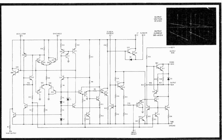
Fig. 8-4. Schematic of the Motorola Phoenix vertical output subsystem on
a single IC chip. Waveforms show voltage and current outputs. (Courtesy Ben
Scott)
MOTOROLA IC VERTICAL DEFLECTION SYSTEM
The designer of this all-integrated circuit deflection system (Fig. 8-4) was Milton Wilcox of Motorola's Phoenix semiconductor facility, recipient of the Broadcast & Receiver IEEE Group's best circuit award in 1971. In it he does a number of unusual things:
1. Eliminates the feedback loop from the output to the oscillator, which inevitably results in control interaction and affects interlace.
2. Eliminates transformer output coupling, thereby having the drive circuits deliver a restricted voltage across the scan (yoke) coils for a linear sawtooth current, with the current dependent on the coils' impedance.
3. Gives the output circuit an open-loop output impedance to avoid including the usual thermistor and linearity control.
4. Includes a flyback generator to supply a fixed voltage pulse that also can produce vertical blanking.
5. Puts the entire assembly on a monolithic chip in an in-line plastic 675 package, 14 pins (4 used by the heatsink), 0.725 inch long by 0.255 inch wide.
The schematic, with output voltage and current waveforms, is shown in Fig. 8-4. The sawtooth oscillator is biased by Z1, Q28, D1, and D2, and has a single external capacitor (not shown) used for timing connected between pin three and ground.
During scan time, this capacitor is charged by current source Q25 to the point that differential amplifier Q33 through Q36 is switched by an incoming negative sync pulse at the sync-hold terminal, pin 2. This latches Q37 and Q38, turning on Q6, while turning off Q5 and Q7. NPN current source Q3 discharges the external capacitor, forming a sawtooth voltage. This is the flyback part of the IC operation. Vertical scan commences again as differential amplifier Q29 through Q32 switches, turning on Q2 so that it, in turn, shuts off Q37 and Q38. The output is delivered through Darlington stages Q39 and Q40 at the collector of Q1 as a ramp (or sawtooth). The positive ramp from the external capacitor is used during forward trace, while a pulse generated during retrace controls the flyback.
During flyback, a capacitor connected between pins 9 and 12 is charged by the Q8-Q9 current source through diode D4, an external diode from pin 9 to the power supply. When the cycle begins, Q8 and Q9 are off, and Q15 plus Q19 clamp the bases of Q16 through Q18 to ground. Peak current now flows out of the yoke to the supply through D3, D4 and Q23. As the yoke current reverses, Q23 and Q24 clamp the negative side of another external capacitor (not shown) to the supply voltage, while Q21 and Q22 saturate with the coil current increase.
During flyback, D4 (external) is reverse biased and so a flyback voltage higher than the supply voltage develops at the scan coils. This is the boosted voltage for the output.
The output circuitry consists of driver Q13, Q14, Q16, and Darlington outputs Q21, Q22, Q17 and Q18. An oscillator sawtooth is applied at the input-height connection pin 7 (Fig. 8 4, a 90-degree color application ), sending Q13, Q14, Q17 and the associated transistors above into conduction. At the beginning of scan, Q16 through Q18 are turned off, and Q21 and Q22 are fully on, delivering peak current across R28 because of the bias delivered by R26, R27 and R29 from the output bias at pin 14. Meanwhile, the input quiescent voltage is set by resistors R14 through R16, at the base of Q11, Q12, then to Q13 and Q14 by way of a second divider, R17 and R18. A voltage is then ...
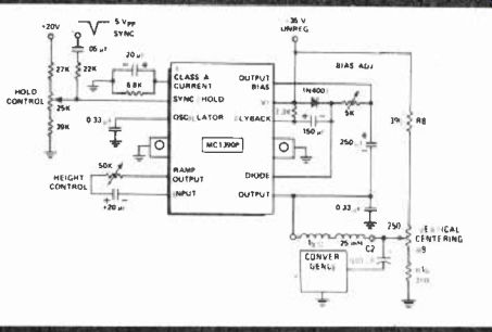
Fig. 8-5. Application drawing of Motorola's MC1390P 90 degree vertical deflection
module.
... developed across R24 in the Q18 output that sets the Class A quiescent current shown at pin 1 with a 6.8K resistor to ground and a 20-mfd filter. If there are unwanted variations, Q10 conducts and regulates any excess current, while an external resistor between diode pin 9 and output bias pin 14 determines the Class A current in Q21 and Q22. Q20 is a short circuit protection transistor across the top half of the output.
As scan continues, Q17 and Q18 begin to conduct, lessening the output current. Q16 also becomes active, shunting current from the upper bias network, diminishing its flow through the bias resistors, and reducing IR drops. Therefore, Q21 and Q22 produce less output. Current now is increased through Q17 and Q18 until, at the center of forward scan, currents equal the Class A current and no output current flows.
With further scan, Q21 and Q22 are gradually brought toward cutoff, while Q17 and Q18 conduct harder until, at the end of the scan, these two transistors are actually removing I peak due to voltage developed across R24. However, Q21 still follows the lower group of output transistors, and so continues to offer a high output impedance. I peak must flow through the upper stages at the beginning of the scan and through the lower stages at the end of the scan. For higher deflection currents (110 degree tubes) and low-impedance scan coils, two XC1390 ICs may be placed in parallel to deliver scan currents up to 2 amps p-p.
ZENITH'S DISCRETE & THICK FILM VERTICAL DEFLECTION
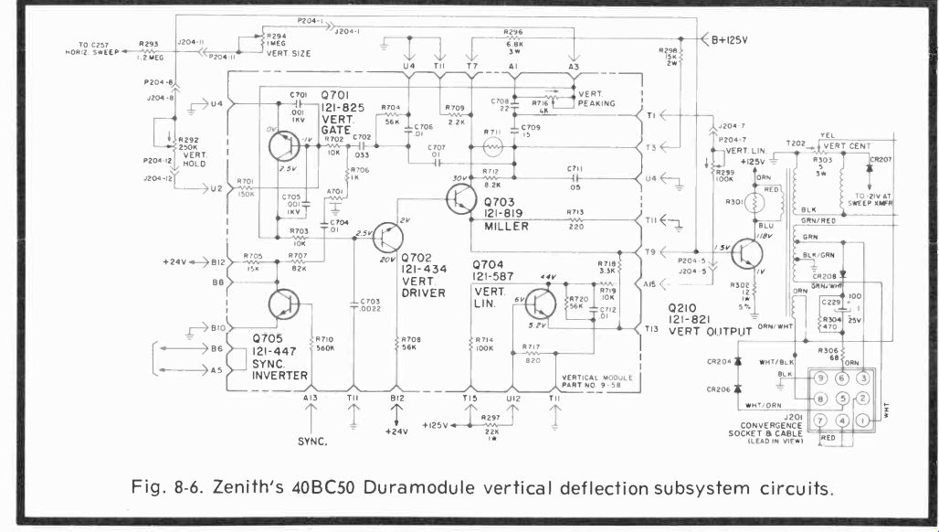
Fig. 8-6. Zenith's 40BC50 Dura-module vertical deflection subsystem circuits.
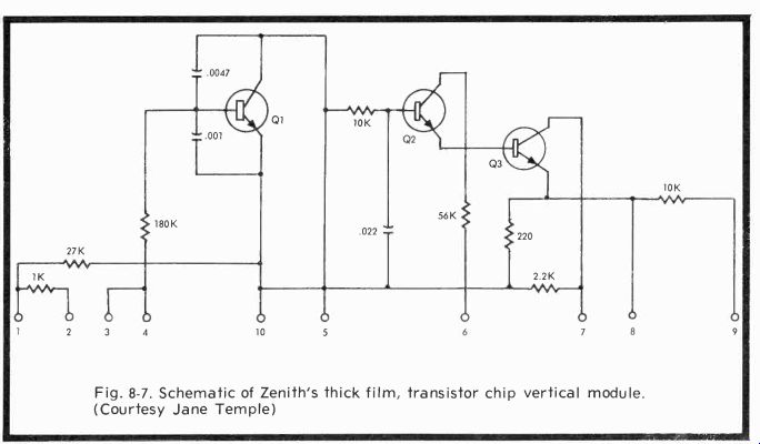
Fig. 8-7. Schematic of Zenith's thick film, transistor chip vertical module.
(Courtesy Jane Temple)
The original Zenith vertical deflection subsystem circuit for the solid-state 40BC50 is illustrated in Fig. 8-6. Sync inverter Q705 inverts the negative-going sync signal so that it turns on NPN gate Q701 during the sync pulse interval, which lasts for the 1.4-millisecond vertical blanking interval.
Collector potential for Q701 and the base drive for Q702 are supplied through vertical size potentiometer R294, with vertical peaking connected to this same line and also to capacitor C708 in the collector of Q703, the Miller amplifier.
And connected between C708 and C709 is one end of the vertical linearity control; the other end goes to the collector of vertical linearity Q704 to shape the output during scan time for the best rising forward trace.
The vertical size potentiometer's source voltage comes from a rectified pulse from the flyback transformer, so that any change in the pulse amplitude will affect the vertical size and cause it to track with the horizontal. Q702 also receives drive from the sawtooth developed by the Miller amplifier through C708 and the vertical peaking control. Q702 is DC emitter-coupled in phase to the base of the Miller amplifier.
Output of the Miller stage is emitter-coupled to the base of the vertical output. Another output from collector feeds the base of Q701 through C707, C702 and R702. Also, the Q703 output takes its Miller route through C708 and C709 to the base of the vertical driver. The thermistor takes care of temperature changes by proportionally increasing or decreasing in resistance.
As the receiver is turned on, C702, C706 and C707 are charged through several paths from B+, while Miller capacitors C708 and C709 wait for charges that take place only during retrace. This is because the Miller oscillator is not conducting at turn on and the collector voltage goes to almost full DC-the point where C709 and C708 take on full charges.
With Q701 in saturation, the charge on C702 is dissipated, and Q701 comes out of conduction. Capacitors C708 and C709 then take over and begin to discharge during forward trace time, turning on Miller amplifier Q703, which further discharges C708 and C709. The positive sawtooth present in the emitter of Q703 is applied through the vertical hold to the base of Q701, and the vertical hold and C702 form a time constant that both restarts the entire process and also keeps the oscillator operating when there is no incoming sync pulse. Vertical peaking, naturally, affects the discharge waveform (undoubtedly, its symmetry), while the vertical linearity transistor is something of an active circuit that could change with variations in DC, preserving sweep symmetry by a second method.
There is another version of the same circuit that includes most of what is shown in Fig. 8-6, except sync inverter Q705 and vertical linearity transistor Q704. In Fig. 8-7, the linearity control is connected directly to the emitter of Miller Q3 through a 10K resistor. There are a couple of other minor changes, but the big point of this illustration is that the revised circuit is also the new thick film transistor-chip module. The final number in the 700 series now corresponds to "our" numbers on the thick film diagram. The 9-751 and the new thick film circuit should be direct replacements. The difference, of course, is that the heart of the new circuit is in a sealed ceramic package and must be replaced in its entirety should there be a fault.
QUESTIONS
1. Name the field scanning rate of the vertical oscillator.
How many fields to a frame? What is the field scan and retrace time?
2. What's the biggest problem in the vertical circuits we're discussing?
3. A tube-type vertical oscillator delivers what kind of a waveform to the vertical output? The transistor oscillator waveform?
4. Pulse-shaping networks in vertical oscillator and output circuits are always what kind of components?
5. Why does the vertical oscillator stay in virtual sync and continue to drive the vertical output when there is no incoming sync signal?
6. What are the advantages of blocking oscillators?
7. What would you expect the Xc reaction of a vertical output capacitor to be?
8. How can the use of a single IC help you troubleshoot an entire vertical subsystem?
9. The two most active capacitors in Zenith's Miller amplifier are?
Next: Link | --Horizontal Deflection System
Also see:
TV Antennas and Transmission lines
Air Time--An Intro to Television Broadcasting
TV and Radio Tube Troubles (1958)