Gates
The gate, or logic gate to give it its full title, is the building block component of digital circuits, rather in the way that the single amplifier stage is the building block for conventional audio circuits.
Gates for digital use come in two main types, called AND and OR, and the action is rather more strictly defined than that of a gate in a linear circuit. Our idea of a linear gate is a circuit that will pass or block a main signal in response to a gating signal on another input, as Figure 2.1 suggests . In this respect, a gate in a linear ...
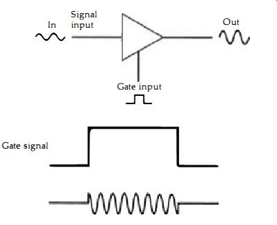
Figure 2.1 The action of a linear gating circuit. The main input and outputs
will be analog signals, with a square-sided signal used to switch the gate
on and off.
The waveshape of the analog signal is preserved, and the only gate law is that the gate is open for a high voltage at the gating input and closed for a low gating input.
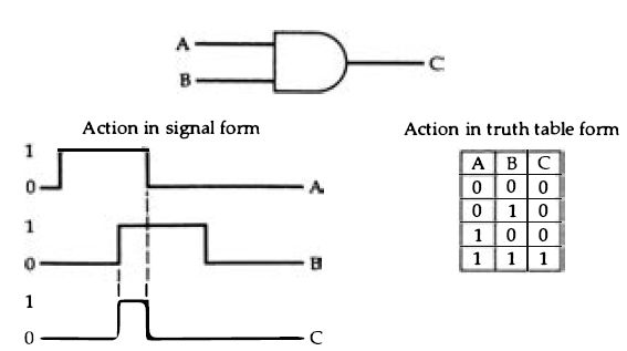
Figure 2.2 The action of the AND digital gate. Inputs and outputs are digital
signals of about the same amplitude, and the output depends on the combination
of inputs. In this case, the output is 1 only while both inputs are at 1.
The action has been shown both in signal form and in the more common truth-table
form.
... circuit is no more than an on/off switch for signals. Though the digital logic gate can also be used in this way, its distinguishing feature is that the conditions that determine the output of the gate obey a set of rules that can be summarized in the form of a truth table, and which are affected by all the inputs to the gate, unlike the analog gate in which one input is of a signal and the other is a gating waveform which determines whether the signal is passed or not.
Figure 2.2 shows a typical truth table along with the conventional symbol for one gate type, the AND gate. These symbols are taken from the international set that are used by manufacturers and users . The important point is that the gate illustrated here has two inputs, both of these inputs are digital signals, and the signal that you get at the output of the gate depends on both of the input signals. Since a digital signal can have two values only, 0 or 1, the table shows only these signals for each possible combination of inputs . As you can see, the output is 0 for three combinations of inputs, and only for the fourth does the output change to 1. This is when input A and input B are together at level 1, and it' s for this reason that the gate is called an AND gate . If three inputs are to be used, the truth table and symbol are as shown in Figure 2.3.
There is still only one condition that results in a 1 at the output --when all inputs are at 1. No matter how many inputs an AND gate is designed to use, then, there is only one combination of inputs that produces a 1 at the output, and that's when all of the inputs are at level 1.
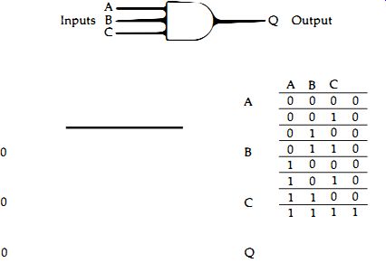
Figure 2.3 The action of a three-input AND gate shown both in signal form
and in truth table form.

Figure 2.4 The symbol and truth table for the NANO gate, which is the equivalent
of an AND gate followed by an inverter.

Figure 2.5 How the NANO gate can be used as an inverter. Any logic system
can be made up from NANO gates (or from NOR gates) alone, so that this gate
is a fundamental building block of digital ICs.
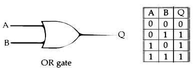
Figure 2.6 The action of the OR gate, illustrated here for two inputs. Note
that this is not our everyday idea of OR, because it includes the case where
both inputs are at 1.
As it happens, it's very much easier to manufacture an inverted form of this gate, known as the NANO gate, and its truth table and symbol are shown in Figure 2.4. The small circle shown here at the output of the symbol means inversion, and the Nin NANO means NOT. The output is 1 except when inputs A AND B are 1, when the output becomes 0. The value of the NANO gate is that it can be used for more than one purpose. Suppose, for example, that you connect the gate in either of the two methods shown in Figure 2.5, using earth to provide logic level 0 and the supply voltage to provide logic level 1. Either way round, the gate acts so as to invert the signal at its input, supplying a 0 if the input is 1 or a 1 if the input is 0. This is just one example of the versatility of this type of gate, and for a full explanation of how it can be used to provide any type of gate action that you might want you will have to consult a book such as my Digital Logic Gates and Flip-Flops (also from PC Publishing) because we haven't space to go into all the byways of gate circuits here.
The other main gate type is the OR-gate, and the symbol and truth table for a two-input OR gate are illustrated in Figure 2.6.
The output from the OR-gate is 0 only when both inputs are zero, and if any one input is 1, or if several inputs are 1, then the output is 1. This is not our everyday sense of OR, meaning one or the other but not both, so some care is needed if you are new to these ideas. Once again, the opposite type of gate is easier to make, and the NOR gate (Figure 2.7) is more usually found in IC form. The ...
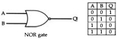
Figure 2.7 The NOR gate, equivalent to the OR followed by an inverter. Like
the NANO gate this can be used as a basic building block of al digital circuits.
... more familiar type of one-or-other action is obtained from a different gate, the XOR (exclusive-OR) whose symbol and truth table is shown in Figure 2.8. This latter type of gate is extensively used in making gate circuits that carry out the arithmetic operation of adding two digital numbers . There is another circuit which is usually included among the gates and referred to as the NOT gate, Figure 2.9. This is a digital inverter and though its action can be obtained from either the
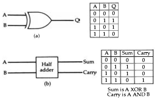
Figure 2.8 (a) The exclusive-OR gate and its truth table. This action is
closer to our idea of OR, because it excludes (hence the name) the case when
both inputs are at 1. (b) How the action of simple addition of two bits can
be carried out by an AND gate and an XOR gate.
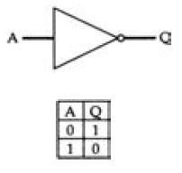
Figure 2.9 The NOT gate symbol and truth table.
NAND or the NOR gate, it is often convenient to use the NOT symbol in circuits to match its important place in digital logic. The significance of the NOT gate is that NOT 0 is 1 and NOT 1 is 0, a vitally important part of digital logic.
The importance of these gates is that they form the main units of any digital system. Any type of logic action can be provided by using gates on digital signals, so that if, for example you wanted to obtain a 1 output when any two out of three inputs were at 1 it would be possible to design a suitable circuit using gates, and it would equally be possible to design the circuit from either the NAND or the NOR type of gates alone. Counting circuits can also be constructed from gates, so that the gate is to the digital circuit as the transistor is to the linear circuit. Knowledge of gates is not essential to the understanding of digital audio, but it's the simplest path into an understanding of the more advanced circuitry that is used in CD players, usually entirely in IC form. The logic actions that are needed for CD use include the track selection, track following, display of track availability, error correction, laser focus control, motor speed control, so that the logic circuits which are not involved directly in the audio reproduction system are nevertheless not exactly unimportant . Though you probably won' t have to design them for yourself, or even service them, it's important to know what is involved, because the essence of gate logic is that any particular combination of inputs will produce an output which can be predicted from the truth table . Because of this, a logic circuit can be checked using DC steady voltages, and --n-0?g elaborate is needed. It's very different when we get to sequential circuits .
Sequential circuits
Gate circuits are sometimes known as combinational circuits because what you get from the output of such a circuit depends on what combination of 0’s and l's happens to be present at the inputs . There is a very different type of circuit that can be built using gates, in which the output depends on the sequence of inputs rather than the combination. The simplest example is a counter IC, in which the state of the outputs will depend on how many pulses have arrived at the input. The classic type of sequential circuit is the flip-flop, though the digital gate version of this circuit is far removed from the simple type of direct coupled multivibrator that may be familiar to you. The most elementary form of flip-flop is known as the R-S flip-flop, and though it has few uses nowadays, it is incorporated into a lot of IC's circuitry, and its action repays study. One type of RS flip-flop circuit using NANO gates, is illustrated in Figure 2.10.
Trying to understand what this circuit does looks at first like a monkey-puzzle. The key to understanding is to remember that the output of a two-input NANO-gate is zero only if both inputs are at 1, and will be 1 for all other inputs. In the circuit of Figure 2. 10, if input R is 0, then, no matter what the signal level is at input S, the output of gate 1 must be 1. This means that if the other input at Sis at level 1, then gate 2 has both inputs at 1 so that its output is also 0. If input S remains at level 1, changing input R to 1 will have no effect on the output at Q, because with the other input of gate 1 at 0, the output of gate 1 will still be 1. The action, then, is that a 1 at one input and a 0 at the other will set the output of the flip-flop one way or the other, and a 1 at each input 'locks' the output, leaving it in the state it had just before the change. This is…
Note: the state R= 0, S = 0 is not used because in this state Q=Q=O, and we normally want Q to be the inverse of Q

Figure 2.10 The R-5 flip-flop, the simplest form of sequential circuit. Unlike
a normal (combinational) logic circuit, the flip-flop output depends on the
sequence of inputs, not the …combination. The R=1, 5=1 state is a store state,
maintaining the outputs at their previous value.
... the essence of a sequential circuit - that the output depends on the sequence of inputs rather than the combination of inputs . The basis of all sequential circuits is the flip-flop, and though simpler types like the R-S exist, the most important type of flip-flop is that known as the Master-Slave J-K flip-flop, abbreviated mercifully to JK. This is a clocked circuit, meaning that the action of the IC is carried out only when a pulse is applied to an input labeled 'clock' . This allows the actions of a number of such circuits to be perfectly synchronized, and avoids the kind of problems that can arise in some types of gate circuits when pulses arrive at different times. These problems are called 'race hazards', and their effect can be to cause erratic behavior when a circuit is operated at high speeds. When clocking is used, the circuits are synchronous, meaning that each change takes place at the time of the clock pulse, and there should be no race hazards. Clock pulses, as the name implies, are generated at precisely equal intervals, usually from a quartz crystal controlled oscillator . The symbol and a 'state table' for a JK flip-flop is illustrated in Figure 2.11. The table is a state table rather than a truth table, because the entries show that it is possible to have conditions in which identical inputs do not produce identical outputs, since the outputs depend on sequence of inputs rather than the voltages of the inputs at any particular time . The inputs are to the J and K terminals, and outputs are taken from the Q and bar-Q terminals . The bar-Q output is always the inverse of the Q output . The table shows the possible states of inputs before and after the clock pulse, showing how the voltages on the J and K pins will determine what ...
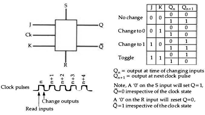
Figure 2.11 The J-K flip-flop. The internal gate diagram has not been shown,
only the conventional symbol. The leading edge of a clock pulse causes the
J and K inputs to be read, and the output changes at the trailing edge of
the clock pulse.
The state table shows how the output will change from 0 or 1 for each possible combination of input at J and K. The J=l, K=l input is called the toggling input and its effect is to reverse the output at each clock pulse.
... the outputs will be after each clock pulse. Note that if both the J and K terminals are kept at level l, the flip-flop will toggle so that the output changes over at each clock pulse, as is required for a simple binary counter . Flip-flops are the basis of all counter circuits, because the toggling flip-flop is a single stage scale-of-two counter, giving a complete pulse at an output for each two pulses in at the clock terminal. By connecting another identical toggling flip-flop so that the output of the first flip-flop is used as the clock pulse of the second, a two-stage counter is created, so that the voltages at the Q outputs follow the . binary count from 0 to 3, as Figure 2.12 shows . This principle can be extended to as many stages as is needed, and extended counters of this type can be used as timers, counting down a clock pulse which can be at a high frequency initially. The type of counter which uses toggling flip-flops in this way is called asynchronous, because the last flip-flop in a chain like this cannot be clocked until each other flip-flop in the chain has changed. For some purposes, this is acceptable, but for many other purposes it is essential to avoid these delays by using synchronous counter circuits in which the same input clock pulse is applied to all of the flip-flops in the chain, and correct counting is assured by connecting the J and K terminals through gates.
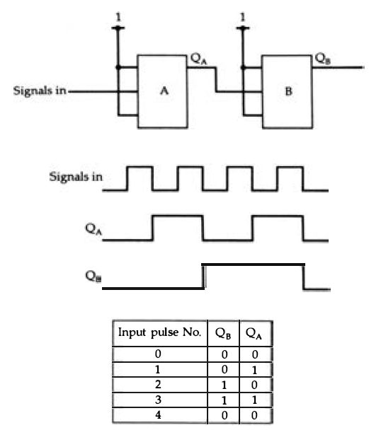
Figure 2.12 How two toggling J-K flip-flops connected together can form a
counter.
The output of the first flip-flop is taken to the clock terminal of the second, so that the second flip-flop is clocked at half the rate of the first. The signals diagram shows the effect of the division, which in terms of 1's and 0’s is a binary count from 00 to 11. Note that flip-flop B represents the 2's figure (the most significant digit) and flip-flop A represents the least significant digit, the 1's figure.
Circuits of this type are beyond the scope of this guide, and details can be found in the book whose title has already been quoted.
Registers
One of the main uses of flip-flops in digital circuitry is to form shift registers, usually in integrated form. A shift register, or more simply register, is an assembly of connected flip-flops and by altering the ways in which the flip-flops are connected we can create four different types of registers. These are known as SISO, SIPO, PISO and PIPO, with the letters S and P meaning serial and parallel respectively, and I and 0 meaning input and output. The actions of these registers are best explained by imagining a simple example of each type, containing four flip-flops with the output of each flip- flop at some level which will be either 0 or 1. The differences are concerned with how the inputs cause changes in the outputs, and the registers are always clocked, so that inputs will cause changes only at the time of a clock pulse, not when an input is supplied . The important feature of any type of register is that it will store digits, because each flip- flop will remain switched one way or the other until it is altered.
The first example in Figure 2.13 is a parallel-in, parallel out (PIPO) register. The flip- flops in such a register are connected only in the sense that the same clock pulse is used for each, but the action of each flip- flop is independent . At the time of the clock pulse, the input is copied to the output, and until the next clock pulse arrives the output remains unchanged no matter how the input changes. You can imagine this used as a sampling device, ...
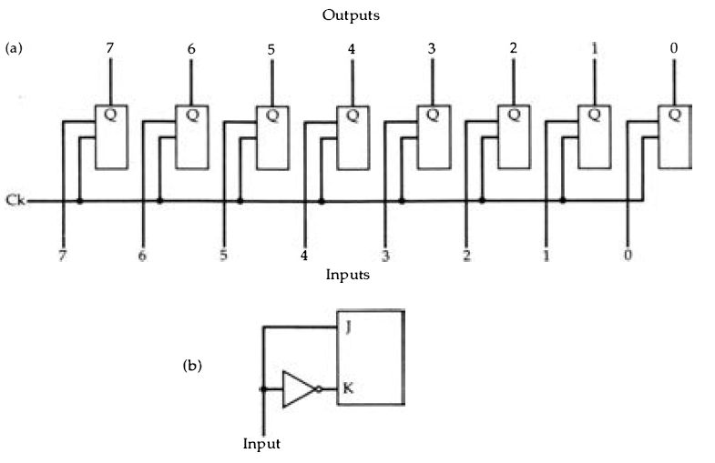
Figure 2.13 (a) Flip-flops used in a PIPO register. The only common line
is the clock line, so that all of the flip-flops copy their inputs to their
output together. Between clock pulses, the outputs remain unchanged regardless
of changes at the inputs.
The numbers 0 to 7 are the position numbers. corresponding to powers of two in a stored number and also to place significance, so that 0 means least significant, 2° (=1) and 7 means most significant, 27=128. (b) The input stage for a J-K flip-flop used in a PIPO register.
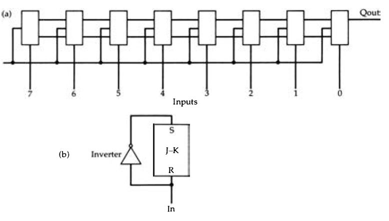
Figure 2.14 (a) The PISO register. The inputs are applied in parallel. one
input to each flip-flop in order of significance. The connection of Q and
Q-bar outputs to the next J and K inputs makes the register into a shift register,
with each bit shifted to the next flip-flop on the right for each clock pulse
. The clock pulses therefore shift the stored bits along the register and
out from the serial output, one bit for each clock pulse so that this eight-bit
register will need eight clock pulses to clear it. (b) How a J-K flip-flop
can be set or reset independently of the clock.
... taking a sample of the input signals at each clock pulse and retaining the sample stored until the next clock pulse arrives.
The second type, shown in Figure 2.14, is the parallel in serial out, PISO type of register . In this type, each flip flop has its own input, but the output of each is also used as an alternative input to the next in line . If we imagine that the register has been loaded by having a set of inputs present, then the action of a separate loading pulse is to make the flip-flops store each input, with the last flip-flop in the register delivering a single bit of output (the same as its input) . Each time a clock pulse comes along, however, the bits in the flip-flops shift one stage along, so that the output delivers the stored bits one by one until the register is empty. This type of register will therefore convert a number code in binary form into a series of digital signals, and this is one crucial stage in converting a digital audio signal into a one-by-one serial form for recording on disc or tape . The serial in, parallel out (SIPO) register of Figure 2.15 performs exactly the opposite action. A set of clock pulses will allow signals presented at the input to be accepted and shifted to the flip-flop

Figure 2.15 The SIPO register. This is also a shift register in which the
bits are written in by clock pulses, eight in this example, and can from then
onwards be read out from the parallel outputs.
Clock Serial out delayed by eight clock pulses Figure 2.16 The SISO register which uses serial input and serial output. A set of clock pulses, eight in this example, will move a bit from the input to the output.
This allows this type of register to be used as a memory in which the first bit in is also the first bit out (a first-in, first-out memory). The main use, however, is as a digital time delay, because the bits are delayed by the time of eight clock pulses.
This technique is used in cross-interleaving (see later). units in turn, so that these bits are available at the outputs . This converts a signal in serial form into one in parallel form, suitable for converting the signal read from a disc or tape into groups of bits that represent numbers.
Finally, Figure 2.16 shows the serial in serial out (SISO) register.
This can be used as a time delay, because if, as in this example, the register consists of four flip-flops, then four clock pulses are needed in order to transfer an input signal bit to the output, with the flip-flops always storing four signals at any given time . The rate of the clock pulse signals will then determine how much delay is introduced, and this is the basis of many types of digital delay techniques used in audio processing, notably in the 'interleaving' process noted in section 6.
Two important features of any IC for digital purposes are the propagation time and the power consumption per device . The propagation time is taken as an average figure for a gate, and means the time between changing the inputs and getting a change at the output. The original types of digital IC (TTL) featured propagation delays of the order of 10ns - one hundredth of a millionth of a second. This order of time is acceptable for all but the fastest circuits, and so newer forms of TTL circuits have aimed at about this same propagation time . To achieve this order of propagation time, the standard TTL circuits used power dissipation figures in the region of 10 mW per gate . This sounds low, but for a device with several hundred gates or equivalent circuits, the power consumption could be difficult to dissipate, and resulted in the chip running hot. The problem with the original type of design was that power dissipation and speed were connected - any reduction in one could be achieved only at the expense of the other.
The conditions of use for digital circuits can be quite stringent, depending on the type of circuit . For some types, the supply voltage has to be maintained at 5.0V, with a tolerance of about 0.25V and an absolute maximum voltage of 7.0V. Each time a gate changes over, a voltage spike will appear at the supply terminals because there is a very brief short-circuit during switch-over. This voltage spike can cause problems in other digital circuits, and so the 5.0V supply should always be stabilized. In addition, it is good practice to connect a capacitor of about 10nF between the supply and earth pins of each device, though if low-power devices are being used this can be relaxed to one capacitor for each five devices . The capacitors are particularly important in large circuits in which there may be long paths from the voltage regulator IC to the TTL circuits. Later types of IC have reduced the importance of the supply voltage and also reduced the amount of spike waveform, but the decoupling capacitors are still important.
The propagation times for digital circuits are affected by temperature, and by the types of load that can be connected. The worst type of load is a capacitive load with a pull-up resistor which is included to ensure that the voltage level rises to about supply voltage level, as illustrated in Figure 2.17, because to reduce the …
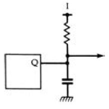
Figure 2.17 The worst type of load for a digital circuit, consisting of a
pull-up resistor and a large stray capacitance.
... voltage of this output to logic 0 means passing enough current through the resistor and also discharging the capacitor, even if the capacitance is only stray capacitance . The switching speed of the circuit will be affected by the amount of capacitance, typically by about 7ns for 80pF. This switching speed may also be affected by changes of temperature, but the effect of temperature is comparatively small . The noise immunity of a digital circuit is an important feature, because it is a guide to what amplitude of interference may cause erratic operation of the circuits. Noise immunity is often quoted in terms of the size of interference pulse that will just cause a circuit to switch over. For many types of digital circuits, the noise immunity is determined by the small difference between 0 and 1 levels . If, for example, the maximum logic 0 voltage of 0.8V is used, and if the gate actually switches over at 1.4V (a fairly common figure), then an unwanted pulse of 0.6V will be enough to cause trouble. This makes some types of circuits, notably the older TTL types, very susceptible to interference on the supply lines, and is another good reason for using capacitors across the supply and earth terminals of each device.
CMOS ICs
The acronym CMOS means Complementary MOS, and complementary in this sense means that MOS transistors with both types of channels are used in pairs. A typical MOS circuit will use a P-channel FET in series with an N-channel FET, as illustrated in Figure 2.18. In this simplified basic circuit, the gate terminals of the FETs are connected together, so that an input signal, which will be a digital signal, will be applied to both gates. If we imagine p-channel FET ...
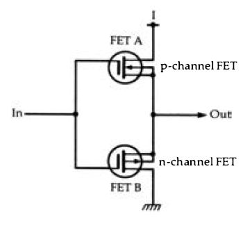
Figure 2.18 A typical MOS circuit element n-channel FET consisting of FETs
of opposite type connected in series. For a digital input, one FET will be
conducting and the other cutoff.
... that the input signal is at logic 1, then the result will be to make FET A conduct fully, and FET B cut-off, with the result that the output is connected to the supply line at voltage level 1. If the input to the gates is at level 0, then the FET A is cut off, and the FET B is fully conducting, connecting the output to zero voltage, logic level 0. The basic circuit illustrated here is therefore one whose output is a replica of its input, neither inverting nor carrying out any other type of gating action. A circuit of this type can be used as an 'expander' , allowing a larger number of loads to be driven from a single output.
The advantages of CMOS construction are that a wide range of supply voltages and logic voltages can be used. The standard and LS TTL circuits are designed to be operated with a +5V supply, and this voltage must be adhered to very closely. Most CMOS circuits will operate with voltages as low as 3V, some at 1.5 V. They can also be operated with voltage levels of 12V or more, so that CMOS circuits can be used with low-voltage battery power equipment, and also can be applied with the voltage levels that are encountered in a car. The switching is also to 0 and 1 levels that are very close to the supply voltages. The construction of the output stages of TTL circuits makes it difficult to achieve a voltage for logic level 1 that is close to the +5V supply level, and which is more likely to be typically around 3.5 V. This makes for a rather poor noise immunity for TTL, and because CMOS can achieve logic levels which are almost equal to the supply voltages, the noise immunity of CMOS can be very much better than that of standard or LS TTL. In addition, the power consumption of CMOS can be very much lower than that of TTL, of the order of a microwatt per gate.
The disadvantages of CMOS at one time were the slow operating speed of some early types, though this is not totally inevitable, and the need for electrostatic protection. The typical propagation time for the older type of CMOS gate is between 100 and 200 ns, ten times as much as the average time for the TTL type of gate. For many applications, this is of no importance at all - the time that is needed for a pocket calculator to work out an action is seldom found to be too long. Where the speed of older CMOS designs may be found unacceptable is in large circuits in which many actions have to be performed in sequence, so that the slow speed of CMOS will greatly increase the overall time . The requirement for fast clock rates can also be a problem - and this is the main problem as far as digital audio is concerned. Modern CMOS devices can, however, be manufactured with very much higher operating speeds, and we can also use devices in which the MOS channels are of the same polarity, such as PMOS and NMOS, which switch much faster than CMOS. The need for faster CMOS has been made necessary by the need for some memory chips in computers that can use very low power, and retain data when operated from a low-voltage battery.
In the early days of CMOS, electrostatic damage caused a lot of problems . The gates of MOS devices are so well insulated from the channels that even a tiny amount of electrostatic charge would not be discharged quickly, so permitting a build-up of voltage. At the same time, the very thin insulating layer of silicon oxide was easily punctured by excessive voltages, of the order of 20V or less in some cases. This means that handling a MOS device, or rubbing the pins against any insulating material or against textiles could cause total and irreversible breakdown of the gates. This looks as if it might be a considerable problem for anyone servicing digital equipment, but by the time that CMOS ICs were being used in any numbers, the circuits included discharge diodes at the gate terminals that ensured voltage limitation.
The important point to remember, though it is never mentioned by the manufacturers of 'anti-static' aids, is that only voltage between the gate and the channel can cause damage. It is possible that by walking across a nylon carpet, your hands can be at 15kV or more, but if this voltage is applied to both gate and channel, it does no harm. ICs that are correctly connected into a circuit are therefore immune from these static problems, because the circuits will have some resistance connected between gate and channel connections that will safely limit any conceivable electrostatic voltage. In other words, static should not cause any damage to a working circuit, whether switched on or off. The only possible case in which damage can occur in normal use is when one pin of a MOS IC is earthed and another pin touched, and even in this case, the built-in diodes should be able to cope.
In many years of handling MOS devices, I have never had one damaged by static, even on days when walking across the carpet and touching a radiator would result in a numbing shock. Figure 2.19 lists the standard precautions for handling MOS devices.
These err, as always, on the safe side, and the precautions that are used in some assembly lines (earthed metal manacles for anyone handling MOS chips, for example) are not mentioned because they apply to specialized situations only. If ICs are never inserted or removed until equipment has been switched off and all voltages discharged, if ICs are kept in their protective packaging when not ...
1. Keep all MOS devices in the manufacturer's packing until needed.
Try to avoid touching leads or pins.
2. Short circuit pins/leads together while installing, if possible.
3. Never allow a gate input to become open-circuit.
4. Use earthed soldering irons and earthed circuit boards while installing.
5. Ensure that circuit boards contain resistive paths between gates and other terminals (drain or source).
6. If devices have to be handled, ensure that surroundings are suitable - high humidity, no carpets of synthetic fibers, earthing on all metal surfaces. In severe conditions, earthed metal clamps may have to be fitted to the wrists of anyone handling MOS chips.

Figure 2.19 The precautions which are urged on users of CMOS and other MOS
ICs.
... in use, and if minor precautions are taken against static, like working with the hands slightly damp and with all circuit boards earthed, then problems due to static are most unlikely.
Figure 2.20 shows the general form of a CMOS gate. The input is always to gate terminals, and the output is taken from one drain and one source. Because the gate terminal of a MOS IC does not require current, the number of gate inputs that can be connected to a gate output (the fanout of the gate output) is limited only by the capacitance of the gate terminals. In other words, if the operating speed is very low, the fanout is almost unlimited, but for the higher operating speeds, the amount of current that has to be supplied in order to charge and discharge the gate-channel capacitance will be a limiting factor. The presence of the protective diodes also increases the amount of DC current leakage, though by a very small amount.
Though CMOS forms one important class of digital ICs, notably for its very low power consumption, many digital ICs use MOS FETs of one channel type only, such as NMOS and PMOS. These ICs offer low power consumption, though not as low as that of CMOS, along with fast operation. These types of FET ICs are used extensively in computing, both for microprocessors and for the supporting memory chips. These and CMOS ICs are also used in a variety of other applications for instrumentation and communications . Many of these ICs are of familiar digital types, such as counters, but with a greater degree of integration. Others are of a very specialized nature, like the speech chips that can be incorporated into equipment to permit spoken messages to be delivered, and the chips that form the signal-processing parts of compact disc and DAT systems . Many of the P-MOS and N-MOS ICs are intended for computing uses, and the popular microprocessor types are included in this heading. In this category of assorted circuits, we also have the 'bucket brigade', which is a type of register, a string of flip-flop devices in which data is shifted from one device to another in a chain at each input (clock) pulse. This device allows information to be delayed by a time that depends on the frequency of the clocking pulses, and the main uses are in obtaining delays for audio systems such as public address, music reverberation and special effects . The same principles, though in much more refined form, are used in the CCD (charge-coupled device) type of light-sensitive arrays that are replacing vidicon tubes in miniature TV cameras and camcorders.
Memory ICs
One very important class of MOS ICs for computing use is the memory type of IC. Memory in computing terms means the ability to retain logic 0 or 1 signals for as long as is needed, and the two classes of memory are volatile and non-volatile. Volatile memory is any type that requires a power supply to be switched on in order to retain data . All electronic memory is of this type, though some CMOS memory can be arranged to retain data almost indefinitely with the help of a miniature battery that is built into the circuit; sometimes a large-value electrolytic capacitor, typically 3F3, can be used for maintaining memory during power interruptions . The true non-volatile memory will retain data with all forms of voltage supply switched off. The most widely used form of non-volatile memory is the magnetic type, and the older type of large (mainframe) computers used tiny rings or cores of magnetic material, each one retaining one binary digit (or bit) . For storage outside a computer, magnetic tapes and discs are used, and a more recent development is the optical type of disc as used in the CD system. The advantage of the CD type of disc is that a very much larger amount of data can be stored in a very compact form and with no risk that the data can be erased by careless exposure to magnetic fields, or by clumsy handling. It is no exaggeration to say that the impact of compact discs on computing is even greater than on audio, because it makes it possible to have huge amounts of data available for a modest-sized desktop computer . The likely impact of DAT (in whatever form it eventually becomes acceptable) is greater still, because unlike CD, DAT can be recorded as well as replayed and the system is ideally suited to backing up the data stored on a high-capacity hard disc in a computer.
Memory for short-term storage can use volatile memory, meaning devices like flip-flops that can store data only while a power supply is maintained. The types of volatile memory are classed as static or dynamic, and the two are radically different.
Static memory (usually referred to as static RAM, because access to the memory can be random, to any part of the memory) makes use of a flip-flop for each bit that is to be stored. Since a flip-flop consists of two transistors, one of which is passing current while the other is off, each flip-flop in a memory of this type will pass current whether the bit that is stored is a 1 or a 0. Very early types of memory of this sort used the flipflops in a chain, clocked so that each clock pulse would shift each bit of data to the next flip-flop in line . This made for a very simple type of memory system consisting of just one flip-flop for each bit, but with limitations to access . For example, 1000 bits of data would be stored in a memory, assuming that it had at least 1000 flip-flops available, by applying the bits to an input along with a clock pulse for each input change . If the data was needed again, it had to be obtained at the output end of the chain, one bit for each clock pulse. A system like this is called first-in first-out, or FIFO memory. Each time the data is read out it must also be placed back into the flip-flops again if it is to be held for further use . In addition, all of the data has to be read - it is not possible to read the 56th bit without reading the first 55, for example, and if you need to keep the data then reading and writing must be carried out together . Developments in IC techniques soon made it possible to connect inputs and outputs to any of the flip-flops in a chip. This is called 'random-access', and the name of random-access memory (RAM) was applied to such a chip to distinguish it from the earlier types . Random access demands the use of large numbers of gates on the chip, and also some method of selecting which flip-flop is to be accessed. The method that is used is to apply binary signals to address pins. The address of a bit is its reference number, the number of the flip-flop in which it is stored. When this number is selected by applying the binary signals for the number to a set of address pins on the chip, the correct gating is selected to make connection to that flip-flop, either for reading or for writing. The basic type of one-bit RAM chip therefore consists of one input pin, one output pin, a read/write pin, and a number of address pins . The use of 16 address pins, for example, allows 2^16 = 65536 different flip-flops to be accessed, so that this number of bits can be stored.
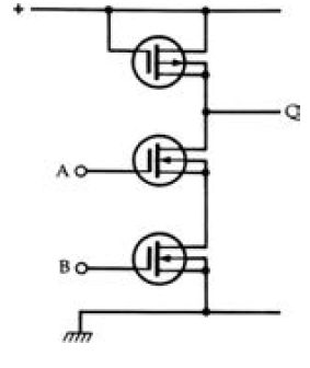
Figure 2.20 A CMOS NANO gate, illustrating that the inputs are always to
the gates of the FETs, so that the input impedance is very high. The output
is always from a source or drain, making this impedance fairly low and so
allowing any output to drive a large number of inputs that are connected to
it.
Any one flip-flop can be accessed by using its particular address number in binary form on the address pins. The use of flip-flops requires current in each flip-flop, and early types of static memory required a considerable amount of power. This led to the development of a different memory type, the dynamic memory, and though CMOS static memory can now be obtained with very low power consumption, the use of dynamic memory is now very well established, particularly in small computers . The principle of dynamic memory is storage of charge in a tiny capacitor constructed like the gate of a MOS transistor. Though the resistance between the contacts of such a capacitor can be very high, the small amount of charge that can be stored, along with the leakage through the selecting circuits of a memory chip limits the storage time to a few milliseconds only. This means that each tiny capacitor that stores a 1 must be recharged (or refreshed) at intervals of, usually, one millisecond. This is not so difficult as might be imagined, because the memory chips can be manufactured with the refreshing circuits built-in, and the master control of refreshing can be supplied either from a special controller chip, or in some cases by the microprocessor of the computer itself. The refresh has to be 'transparent' meaning that it should not interrupt the normal computing actions in any way.
The use of dynamic memory greatly reduces the amount of power that is needed for the memory of a small computer, because power is needed only to refresh the charge on the capacitors that are storing a logic 1 signal . The low power requirement makes it easier to build very large-capacity memory chips, so that the spectacular improvement in the memory that is available for small computers has been due largely to the availability of dynamic memory chips in ever increasing sizes. At the time of writing, the largest dynamic RAM in common use was of 1048576 bits . This is described as a 1 Mb chip, one megabit . In computing, 'K' is used to mean 1024 (which is 21 0) and M is 1024 x 1024 which gives the figure of 1048576, equal to 220 . The importance of temporary memory of this type is that it allows digital signals to be stored for processing. There is no need, for example, for the sampled signals to be recorded at exactly the time when they are sampled, and by retaining signals in memory for a time which is more than the time between sampling times, it is possible to compare successive signals. This is important when the sampled digital numbers are replayed because it allows one sample to be compared with another - in normal music, for example, one sample is not too vastly different from its neighbors, but a sample that is incorrect because of a fault on the disc for example will be very different and can be rejected. Such a sample can be replaced by a synthetic one which can be a number midway between the 'normal' samples, Figure 2.21 . Using memory also allows samples that have been taken at the same time, such as samples of two channels of sound, to be transmitted or recorded at different times by storing one for later transmission, and later made coincident again by storing the one that had not been delayed the first time, Figure 2.22. It is even possible to store groups of signals so that they need not be recorded in the order in which the signals arose; this is a very important part of the processing system of a compact disc, as we shall see, because it ensures that a fault will not affect more than a very insignificant portion of a piece of music . In addition to this temporary memory which may be needed for short-time storing of signals we need a permanent memory system. We want, for example, to keep the signals that make the system work in some permanent form, because a digital audio system would be unacceptable if we had to start it working by feeding instructions into it from a disc, as we do with most types of computers . Memory of this type is referred to as ROM, read-only memory, and it can be of several forms . For the operating instructions of a CD player, the contents of the permanent memory will not be liable to any change, since there will be no significant changes in the CD system in the foreseeable future. The memory can therefore be programmed during manufacture, so that the gates that are operated by the address pin voltage will simply connect the data pin(s) to logic level 0 or 1 directly, not to the outputs of flip-flops or capacitors. ROM of this type is manufactured using a mask during the processing to determine which addresses give 0 and which give 1, so that the complete ROM is referred to as a masked ROM. Masked ROM can be very cheap if large numbers are being manufactured, but for some purposes this is not always possible. If a new and untried system is to be used, setting up for masked ROM could be a very costly mistake if changes are needed. The alternative is some form of PROM (programmable read-only memory), a type of write-once read-often chip. The chips are manufactured un-programmed, but by connecting to an address bus and a data bus, and by using higher voltage supplies than will be used in the computer, the chip can be programmed with a set of 0 and 1 bits . The chip can then be · used like a ROM, but with the difference that since the bits are established by the use of a computer, they can readily be changed if a design change is needed. The most popular type of PROM is the EPROM, which allows the pattern of connections to be made electrically by injecting carriers into a semiconductor, and the pattern can be cleared by exposing the material to intense ultraviolet light, a process called 'PROM-washing'.
Error--Set of samples with error; Interpolation of error
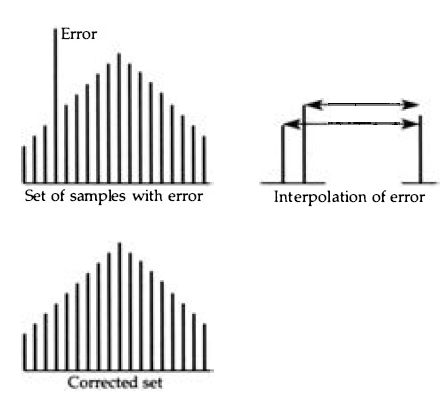
Figure 2.21 Using interpolation to replace a faulty sample with one that
is mid-way between the amplitudes of the previous sample and the following
sample.
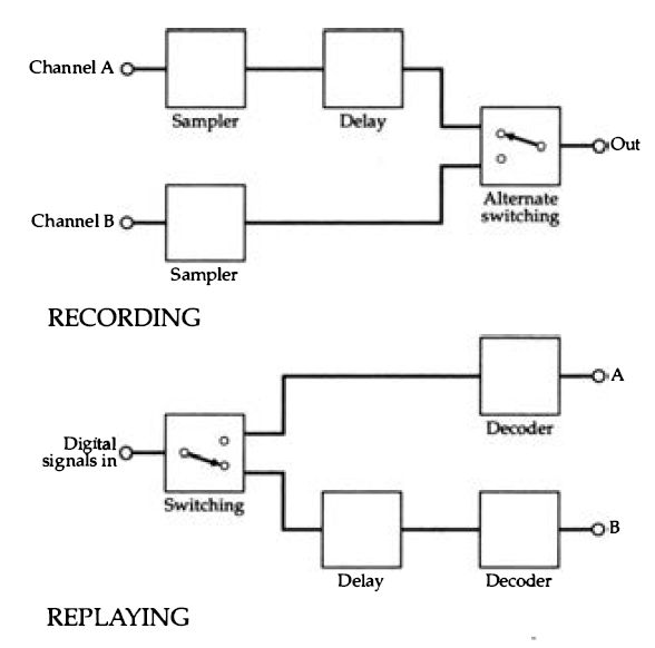
Figure 2.22 Using storage units to convert simultaneous waveforms into alternate
samples and vice-versa.
Microprocessors
The microprocessor chip is the heart of any computer, and is now the universal component of a large number of industrial controllers. The chip consists of a large array of gates and flip-flops, and its unique feature is that internal connections can be made or broken by electrical programming. In other words, a set of binary signals at the data inputs of the microprocessor can be used to set the pattern of gates inside the chip and so determine the action that the chip will carry out with the next set of inputs. The important point to realize is that the microprocessor is a serial controller that carries out one action at a time. For example, if the microprocessor is to add two binary numbers, then it must go through a sequence of actions in which at least three inputs will be needed on the data lines. The first action is to place the ADD command in binary form on the data lines. Following this comes the first of the binary numbers to be added. The next item is the second number, and the output from the data lines will then consist of the sum of the numbers. This makes four distinct steps out of a simple addition, and illustrates why the use of a microprocessor can sometimes be too slow for some control actions . The speed at which the steps can be carried out is determined by a clock pulse rate, usually of several MHz. At the time of writing, speeds of 16 MHz and 20 MHz are fairly common for small computers, and 33MHz is being used on some machines.
Obtaining dock pulses
The final point about digital circuits concerns clock pulses. Most digital systems use clock pulses, and digital audio systems depend very heavily on the use of clock pulses, particularly to maintain the correct sampling rate as we shall see. This leads to the question of how these pulses are obtained in receiving equipment. The two main methods are to use a master crystal-controlled oscillator in each device, or to make the system 'self-clocking' by synchronizing an internal oscillator from sync pulses that are part of the received signal . Computer systems invariably use a master clock, because they must operate for long periods with no incoming data, and are just as likely to be recording data as replaying it. The two methods are not incompatible, and you can find the scheme of using sync pulses to correct a crystal oscillator, as is familiar from color TV circuitry.
Both compact disc and DAT (digital audio tape) use self-clocking methods in which the master oscillator of the replay equipment is kept at the correct frequency and phase by a set of synchronizing pulses that are transmitted along with the audio data pulses. This is particularly important for tape, because the tape can stretch and contract to an extent which would make the use of a separate unsynchronized oscillator impossible . Even discs, however, need self-clocking because of the difficulty of ensuring that a disc is spun with perfect centering and with perfect speed regulation. By using self-clocking along with constant linear velocity (see section 6) such problems become insignificant.